Equites

Robocop repair log #4

 General  Comments Off on Robocop repair log #4
Jan 112019
 

I recently aquired a few Robocop PCBs, and this particular one seemed to be working fine at first glance. Eventually however, I realised that certain sounds seemed to be missing from the attract mode.

In particular I noticed Robocops speech as he rolls off the Prime Directives was not there. A closer look playing the game revealed further sounds missing, like the groans from the enemies as you kill them and others.

I then realised that is was just the ADPCM samples that were missing.

So I looked at the CPU board where most of the final digital and analogue circuits are. First I checked the DACs and found no samples present, so went further back to the large YM2203 sound chip. I probed pin 19 of the IC and would have expected to hear the samples here, however I heard nothing except static.

Pin 19 circled in red

I was able to determine that the ADPCM samples are stored in the EN02 ROM, so I popped this into an eprom reader and checked the content.

The eprom was corrupted, so I burned a new one and the samples were restored.

Another Robocop saved.

Oct 052018
 

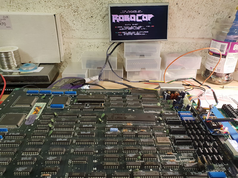
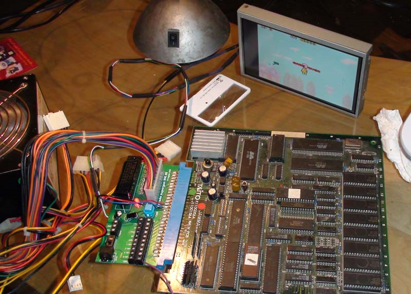
Another PCB which has been collecting dust on a pile. I got myself motivated to repair it.

Symptoms

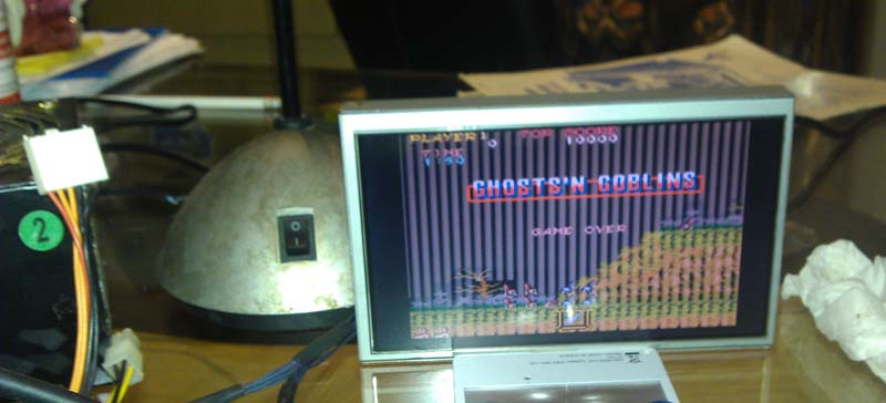
The PCB will not boot, all you see is a white screen.

Decided to check the clock circuit first to ensure the CPU was running, it was, so clock circuit is fine. Next I checked the CPU ROMs, and found a bad ROM at location 8N. Burned a new ROM and inserted it, now game is booting but with issues.

There were absolutely no sprites, and I could not coin the PCB up to start either. The background was full of jail bars.

I first checked the sprite PROM on the A board at 2E, if this goes bad the sprites will dissapear. Both the PROM and socket checked out good. So, my attention turned to the lower B board as this handles all the sprite processing.

It is interesting to note that GnG PCB will boot without the B board but without sprites of course. Handy for troubleshooting.

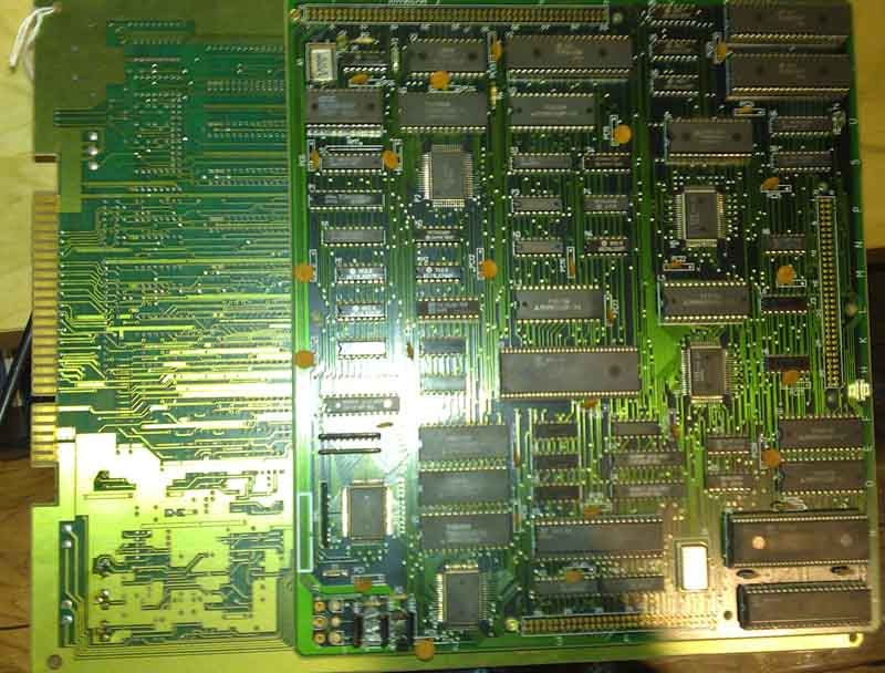
These Capcom PCBs have all the copper path traces masked, obviously an attempt to stop the bootleggers. Luckily, schemes are available, and they are sectioned off into relevant areas of the PCB which is nice.

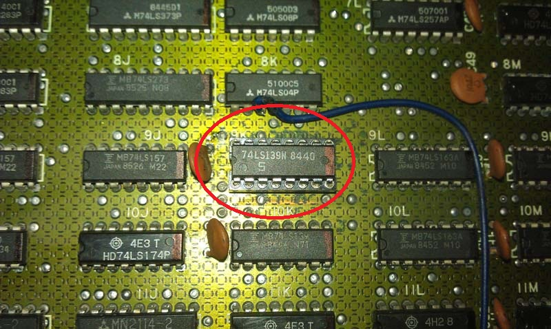
My attention turned to the B board to get the sprites back up. Found a LS139 Decoder IC on the B board at 9K which for some reason was plagued with rust, I checked it and found that it was completely dead, the rust must have worked its way up.

Socketed and replaced it and now we have some sprites which are all wrong, but at least we have sprites.

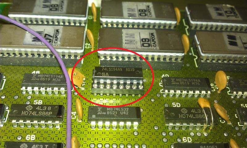
Looked around the graphics ROM addressing circuit and eventually found a LS194 Decoder on board B at location 4C with pins 13 and 14 stuck high.

Socketed and replaced and now the jailbars have gone.

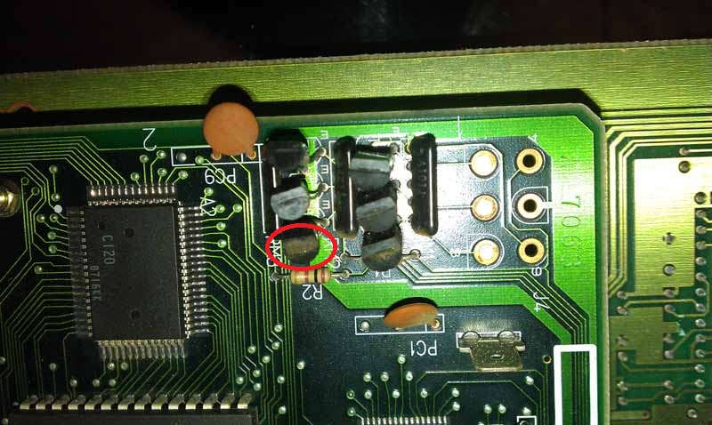
Whilst I was troubleshooting, I noticed that the RED had completely failed and I was left with just BLUE and GREEN, nice! I checked the supergun setup, but no it was the PCB which had failed.

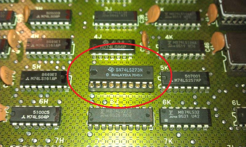
I carried on looking at the sprite circuits and found a LS273 Octal Flip-Flop which had completely failed.

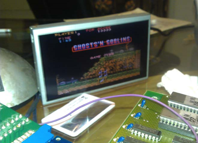
Socketed and replaced it, we now have all the sprites back!

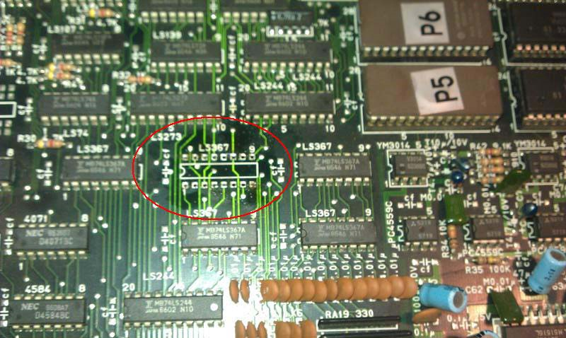
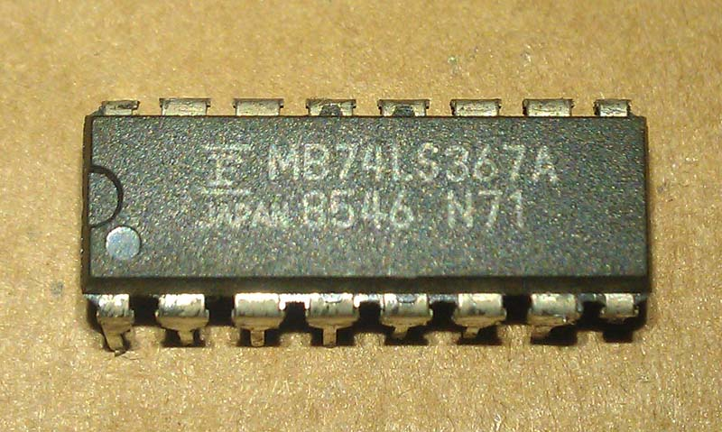
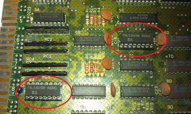
I flipped the PCB over to look at the A board, and using the schemes I could see that a LS367 Hex Bus at location 6C was the final stage for the RED output. I checked it and found that pin 11 was stuck High.

Socketed and replaced it and the RED came back!

Finally, had to resolve the issue of the PCB not coining up. The coin up function works in the same was as the game inputs, so I knew I was looking for another LS367 Hex Bus on the A board. I checked the schemes again and it told me the LS367 Hex Bus at location 8A controlled the coin up input. I checked the LS367 and found pin 4 was stuck Low.

Socketed and replaced it, now coining up.

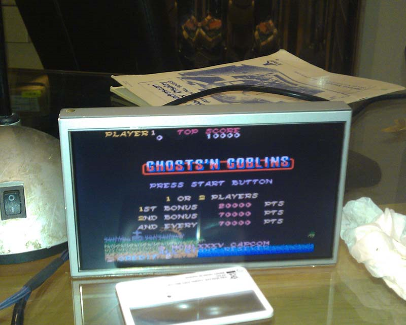
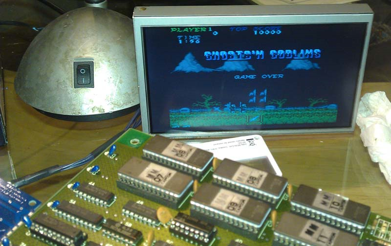
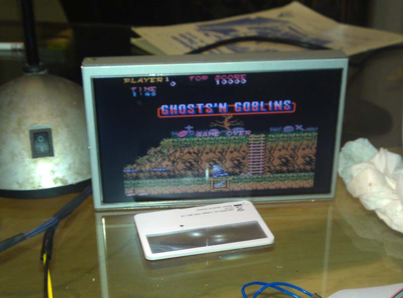
PCB finally repaired.

Galaga ’88 repair log

 PCB Repair Logs  Comments Off on Galaga ’88 repair log
Oct 052018
 

I’ve had this PCB on a pile for nearly two years, decided it was time to look at it.

Symptoms

There is no Green on the graphics, Red and Blue are fine, but colours look washed out because of this.

Started at the edge connector, and using the probe checked the Green pin and it was stuck low, the Red and Blue were pulsing nicely as I would expect.

Traced the Green video path all the way to the second layer which is the main CPU board and smaller. Found a Transistor (TRM3) which had been crushed and legs were shorting, effectively grounding the Green video.

Straightened it out and all good now, full colour is back.

Thing to note is that these Transistor protrude quite a bit, and since these Namco System 1 boards do not have legs, the board tends to sit resting on these Transistors. One to watch out for if you lose a colour on a Namco System 1 board.

Ikari Warriors repair log #2

 PCB Repair Logs  Comments Off on Ikari Warriors repair log #2
Oct 052018
 

Symptoms

The PL1 Ikari character keeps going up on its own when I start a game, the PL2 Ikari is fine.

Looked at my rotary stick, could not see any problems, so I disconnected the sticks from the PCB. The PL1 Ikari character was still going up on its own.

Next I looked at the SNK to JAMMA adaptor, saw no problems here, the fault must be on the PCB.

The PCB is an original SNK three layer PCB set, and uses SNK pinout.

I determined which pin on the edge connector was used for PL1 UP, and traced it back to a SIL resistor array, followed it through a 0.1uf ceramic capacitor where it went to a Hex Buffer 74LS367 at location D4 on the top layer of the PCB stack which handles the joystick inputs.
Bought out the logic probe, and found that Pin 2 (output) on the Hex Buffer was dead. Desoldered it and put the Hex Buffer into my IC Tester which confirmed that Pin 2 had failed test.

Offending Hex Buffer, a Fujitsu branded variant;

Soldered in a new 74LS367 Hex Buffer, all working great now, PL1 Ikari no longer has suicidal tendencies.

The New Zealand Story repair log #3

 PCB Repair Logs  Comments Off on The New Zealand Story repair log #3
Oct 052018
 

Had a look at a Taito New Zealand Story which was not booting for someone.

Symptoms

The PCB would not boot, would be greeted with a BANK RAM ERROR message, then the PCB would attempt to reboot every 5 seconds.

Had a look at this tiny PCB, and noticed it only housed two large RAMs, a 6264 and a 6256 (HM65256B). One must be for graphics and the other program code, I didn’t bother with schemes to check which was which.

The BANK RAM ERROR message meant either a RAM buffer had failed, or one of the RAMs, given that the PCB used a single large RAM instead of several smaller ones, so the message could apply to a single RAM in this case.

Checked the buffers, they checked out good. Then checked the 6256 RAM at location U31 first, good guess as I found one of the data lines was floating using a logic probe.

Desoldered it, socketed the PCB and inserted a new RAM.

All working 100% now.