
Had this guy on the bench for far too long now. The reason? Its a horrible mess of wires used to convert it from something else. Not sure if this was some kind of factory conversion or someone was churning these out at one point in history but its not really something I want to work on again.
So, on power up I get this
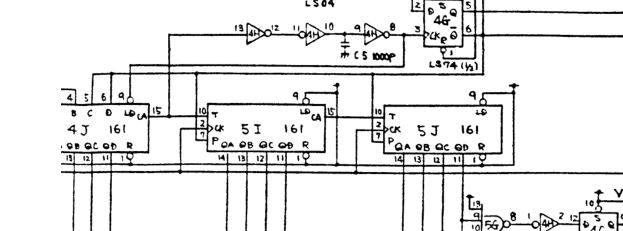
When I first saw this on the video I was sent my first thought was one or more 161 counters had gone bad and then I started looking at the schematics (for Bandido) I found what I hoping to find.
There are actually 4 of these (the other one is on the previous page) so I was half prepared for when the PCB arrived.
When I tested the PCB for myself I could make the issue slightly better with more voltage but never managed to get it perfect within the upper voltage limits.
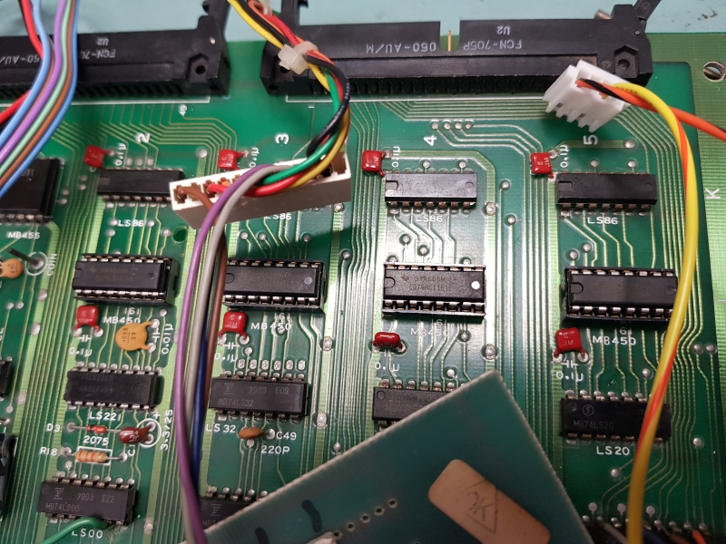
First thing I noticed on arrival was although the schematics were accurate the chip locations were not.
Like I said at the start of this the PCB is a mess of wires which are directly soldered to other parts of the PCB’s which made taking this stack apart a little tricky but needs must so I did.
Finding a bank of four 161 counters was easy enough.
Feeling sure of my diagnosis I removed all four counters and tested them out of circuit but they all passed.
I socketed and replaced them anyway as I know from previous experience these are a fail point.
When I retested the game the graphics issue was now fixed! I could even lower the voltage to 4.8 without problems. I guess these old ones had started to fail and gone out of spec.
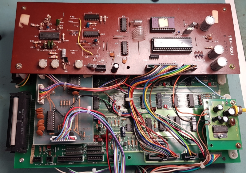
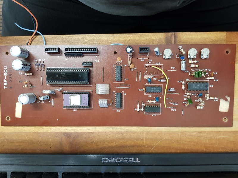
Next issue was the sound but before looking into that I was very curious about the intermediate PCB half hidden under the sound board.
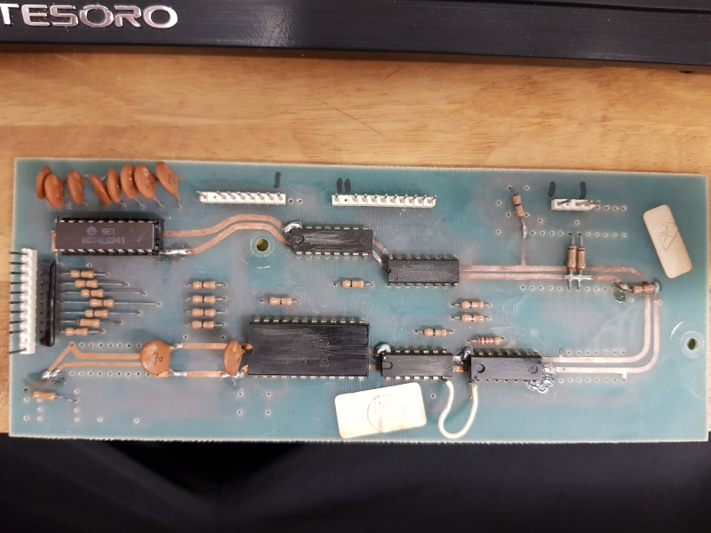
This thing is a horrible freak of nature.
I knew it was something to do with the controls but why so much circuitry? What is that EPROM looking chip on there? and why did it look homemade?
Sadly I don’t know the answer to that last question but I have a fair idea of what the other two are.
First up that EPROM looking thing.
I desoldered it and tried to identify what it was. Best picture I could get from the scratched off markings were this
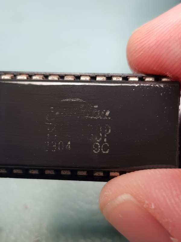
I could see it was likely a Toshiba device and it had “333P” appended so after a fair amount of sleuthing It was deduced that it was TMM333P device.
As I had no way of reading this with any of my programmers I resorted to using the faithful Arduino to dump its contents. After successful extraction it actually identified in MAME as a ROM from Jatre Specter. This made little sense until I traced out the connections and realised it was actually hardwired to address $4E7 so one ever gave out the byte 0x3A. Furthermore only 5 bits of the byte were being used and they are only used to permenantly enable the adjacent logic chips.
My best guess here is the bulk of this PCB is for obfuscation purposes.
On another sidenote, I tried making a small replacement PCB for this using a CPLD and while it worked as expected without the outputs connected it went wrong when they were connected up. Looking on the scope I could see a fair bit of bus contention so I think the CPLD was just too fast for this old hardware.
Anyway, on with the repair.
There was no sound. I started probing around the 8035 and found it was giving out garbage. I pulled the 2708 ROM and found that also full of garbage. I did try erasing it and reprogramming but it wouldn’t program at all. I replaced this with a slightly modified 2732 EPROM.
I ordered a new 8035 and while waiting I decided the best course of action would be to refurb this whole PCB as much as I could. All capacitors were replaced and replaced some of the logic IC’s too just for good measure.
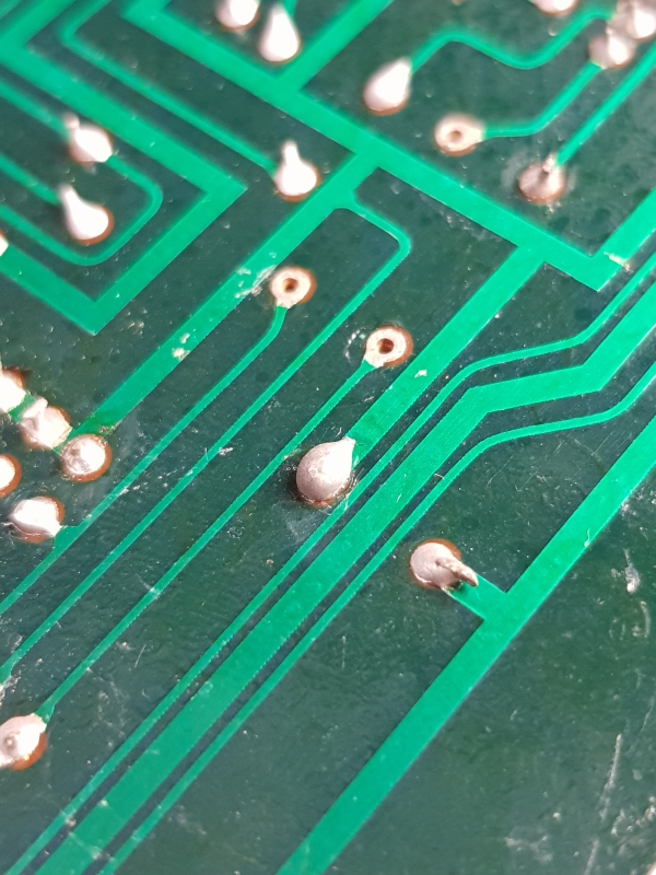
Found a few dodgy looking solder joints like this one along the way
The replacement 8035 came from eBay but it was DOA. The seller send me another no questions asked and this one worked fine.
That’s about it for this one.
Worth noting with this conversion that it was been wired to use the player 2 joystick as the aiming function for player 1.
Sorry, the comment form is closed at this time.