
This one has been fun.
Ben76 on the J+ forums has many sets of Spy Hunter PCB’s but none of them are in working states.
He kindly sent me a board set and a loom of some sort so I could learn a bit more about the hardware and to attempt a fix.
My idea was to create a test rig for this hardware as they seem to be quite prone to failure after their many years of service.
So to start with, as always it was a visual check. The boards, although in need of a clean, were in decent condition.
There was some old flux on the underside of one of the boards that I cleaned up.
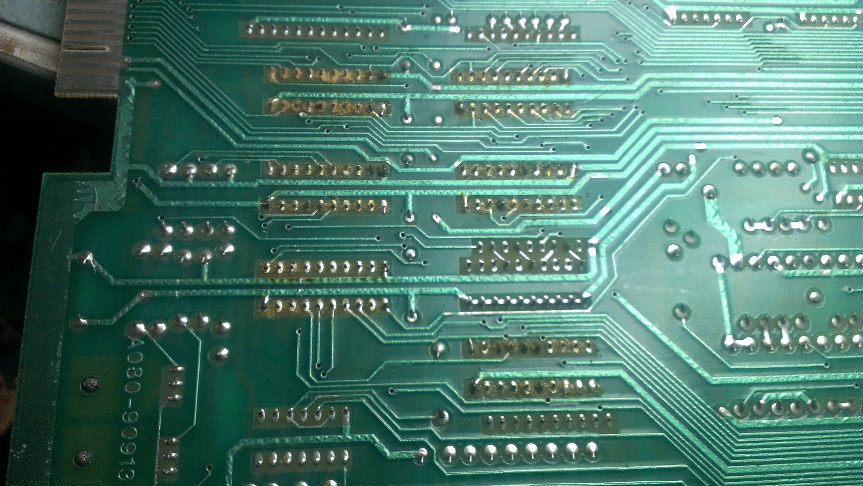
Checked resistances between the power pins to make sure there were no shorts. All clear.
Next was the ROM check and also where the fun started.
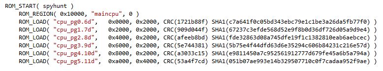
All the ROMs on the CPU board checked out except for the 27128 EPROM at location 11D. My dump also came out half split swapped compared to the MAME dump.
I fitted the Z80 pod so I could use the Fluke 9010.
The first ROM at 6D gave crazy reading, this was sorted by reseating the ROM a few times.
The odd thing was that reading 11D with the Fluke gave me a signature comparable to the one in MAME.
TO THE SCHEMATICS!
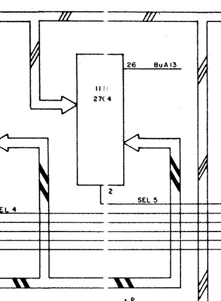
From here you can see that the upper address pin (A13) is connected straight to the CPU (via buffer).
From the MAME driver you can also see where ROM 11D starts.
So, 0xA000 = 1010 0000 0000 0000 in binary which means that when this ROM is read address line A13 is HIGH so the upper half of the ROM is read first.
This has now been rectified in MAME.
One mystery solved.
Since I had the Fluke hooked up I gave the RAM’s a checking over.
Its quite well documented online that the NVRAM can cause issues when booting so lets look into this for a moment.
The NVRAM is used for book keeping and maybe other things too. The RAM chip used is a 6116 compatible RAM which under normal usage is volatile meaning it loses its contents when the power is removed. To combat this BITD a battery was installed in order to keep the RAM chip alive when power was removed. Now we all know batteries don’t last forever and many are either dead or were removed long ago. This wouldn’t normally be a huge issue as for the average collector/gamer book keeping isn’t too important BUT this RAM chip is subject to a RAM test on startup. If the battery is dead or removed then the chip has no power and will fail its RAM test which will result in a non booting game.
The ways around this are either fitting a new battery or you can add a wire link at JW15. This will attach the chip to the +5v line.
To check this RAM with the Fluke this jumper needs to be in place or alternatively if you run the game for a couple of second you can test the RAM then as it will be properly setup.
It is setup by a counter which after a certain number of clocks activates the chip select line. According to Midways own documents this is to ensure proper startup/shutdown of this NVRAM to prevent data loss.
There is a PLD chip at location 1F which decodes these writes to the counter. I have successfully reversed this chip and a replacement can be programmed into a GAL16V8.
Anyway, The RAM’s checked out fine.
Maybe I should try running the game.
Little did I know before taking this on that the game uses HV sync lines instead of composite sync. I initially made up a simple circuit to combine these which seemed to work but my test TV is quite picky about certain sync signals and just displayed a black and white picture. I then recalled that my 1084 monitor can accept HV sync.
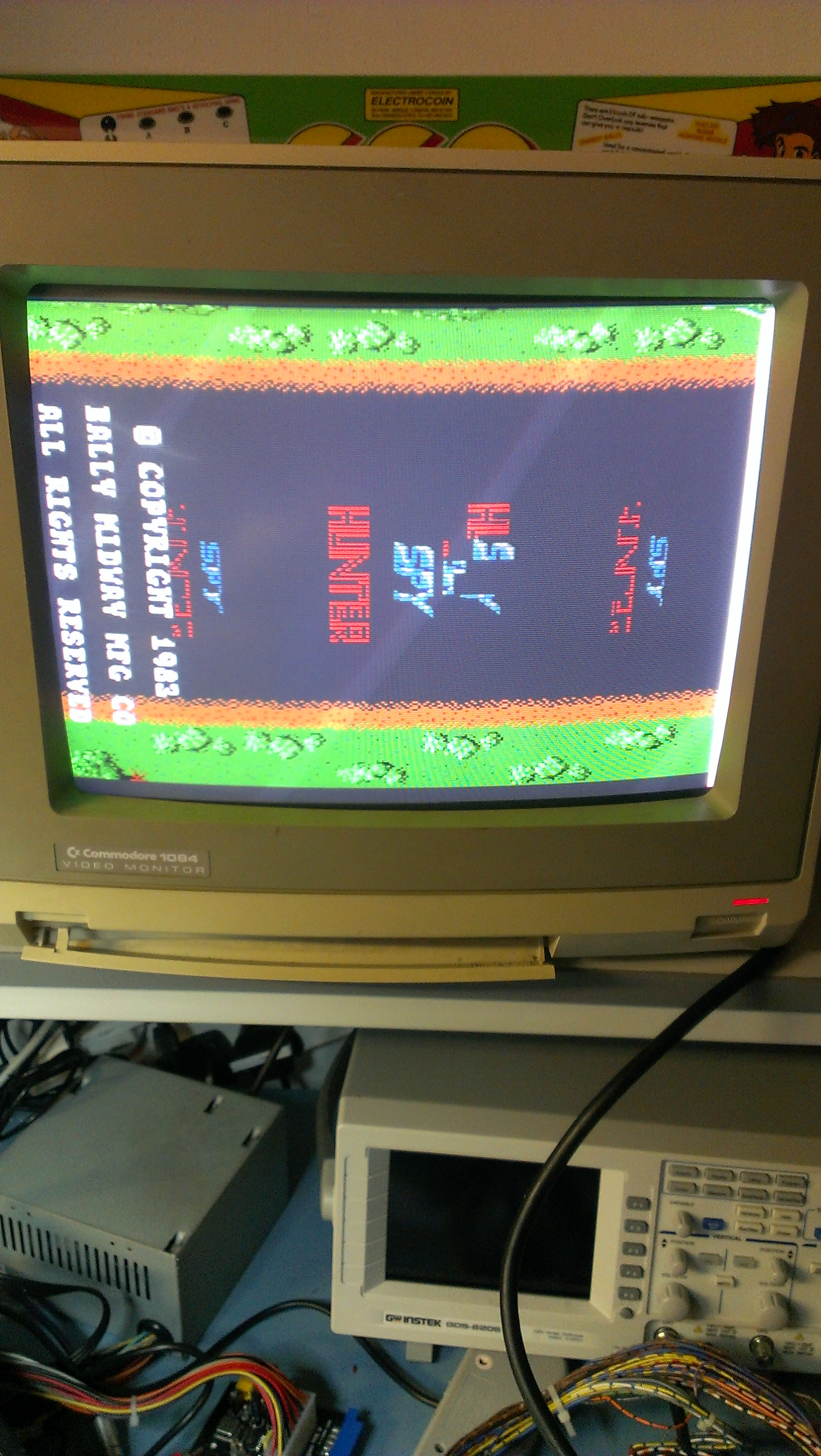
Unexpected to see this working in a fashion. Clearly the graphics are a bit messed up but its playing. The screen is flipped as I did not have the SSIO board attached at the time.
So whats wrong with these graphics.
All the ROM’s checked out fine.
There are a lot of 93422 RAM chips on this board that I cannot test using my usual methods.
The answer was writing my own test program for the Boardmaster 4000.
All these RAM chips tested good.
Feeding the address lines to these 93422’s were a bunch of 74LS169’s. Probing these quickly showed the chip at C12 had some stuck outputs when compared to the rest of them. Replacing this chip cleared up all graphics issues.
Nearly time to hook up the SSIO board. Before doing this I checked all the chips I could. All the ROM’s were fine.
As the SSIO board has its own processor I was able to test this board independently of the others.
With the Fluke attached I could not get a consistent read off the ROM’s.
I found a shorted out 74LS374 @ A5. This chip is the link between the SSIO and the main PCB data lines. With this replaced everything was good.
Now with the SSIO connected the screen flipped but I get the “Sound Board Interface Error”

This “fault” gave me the run around for a week, literally!
It was a issue that I had actually caused in the end as when I removed the ROM’s I didn’t take note of which way around they were. Enter mystery #2.
I went as far as disassembling the code to see why this error is given. Here is what it does.
The main PCB writes data to the audio latches at address $1C-$1F, it then looks for the same data returned on the audio status address at $7
At this time the SSIO reads the latch data, compares it against the values it expects and if all the latches match it then writes the value into the audio status for the main PCB to read.
It does this for several values. If any of the values don’t match or it times out then you either get the “Interface Error” or the “Timeout Error”.
With all this in mind I went about checking this whole circuit. It all checked out fine. This is what led me onto looking at the ROM locations and finding that MAME has these two labelled wrong. They were in the right address space in the driver but the locations for A7 and A8 were swapped in the filename.
With this corrected the error message was gone.
On to the sound itself.
Here is where my main headache happened.
As I was using a switcher there was a lot of noise present on the audio section, so much so that I could not make out any clear unamplified audio signals. At this point I went ahead and injected my own signal in at a point and followed it through.
Right away I found all three of the 4016 chips were burning hot after seconds of power on. I replaced all these.
As I couldn’t get anything at my test speaker I tried replacing the op amps with no luck.
After a lot of patchy testing sessions I just suspected some bad AY-3-8910 chips so ordered a load up.
Before receiving these however I saw that the game uses another PCB. This one is an amplifier PCB.
Taking some advice from Irongiant I butchered the audio cable from a set of powered speakers and hooked them up to the output pins. With the sound test running and the volume turned up to full I could just make out the sounds of the game. This was kind of encouraging as it meant the board was actually running and playing the right sounds.
All I could think of was shotgunning the capacitors and just before placing an order I remembered I hadn’t tested something.
A few days back I posted a message asking if anyone knew what kind of volume I would get out of this if the volume potentiometer wasn’t installed. No one really knew and I forgot all about it.
So before pressing the “Confirm order” button I went and tested the pot 1kohm pot I had ordered. To my surprise the audio was nice and loud with this installed and was fully adjustable.
I coined up the game but was greeted with some odd screens that didn’t match what I expected.
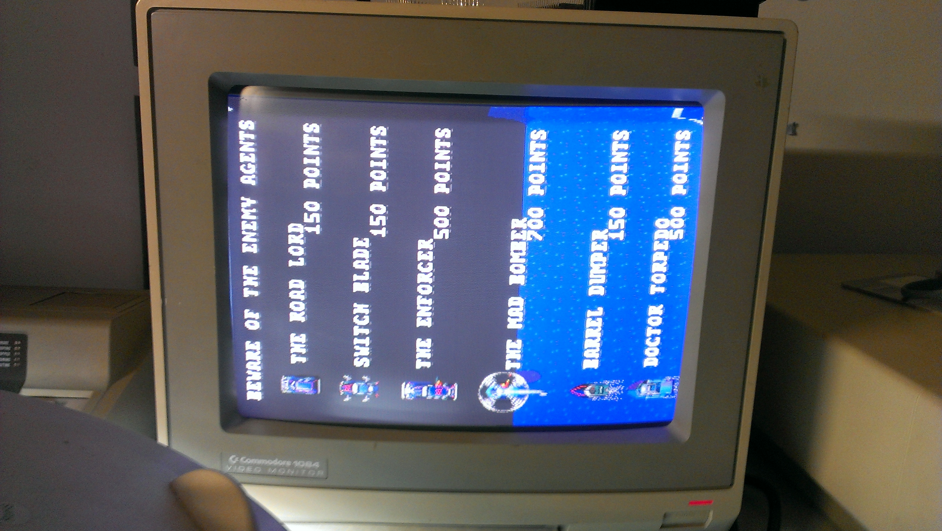
This is one of 3 different screen showed.
After asking Ben he confirmed that if you press the accelerator when it is coined up it will show these screens. Doesn’t explain why they were so messed up so checked in MAME and they too were a bit messy looking.
Entering the test menu and poke about the pins to get the values for the accelerator to change so I am confident they work to some degree but I cannot test the player controls any further.
When I start the game the car accelerates off and to the left causing it to die immediately.
This kind of concludes my testing of this board set.
I would also like to thank the following:
Ben76 for sending me this stuff
David Haywood/Phil Bennett for their help in confirming my issues with the ROM’s
Irongiant for putting me on the right path with the sound
Equites for his kind offers of parts if I needed them
Frothmeister also for his kind offer of parts
anyone else that has helped or provided any input what so ever
4 Responses to “Spy Hunter repair log #1”
Sorry, the comment form is closed at this time.
Thanks loads 🙂
Just wanted to let you know how much I appreciate all the sharing of knowledge. The time you invest to write this all down to allow us to enjoy and learn is quite extraordinary. THANKS!
Very welcome. Thanks for taking the time to comment and of course thanks for visiting.
Fantastic detective work there, Sherlock };-P
And as always nice reading…