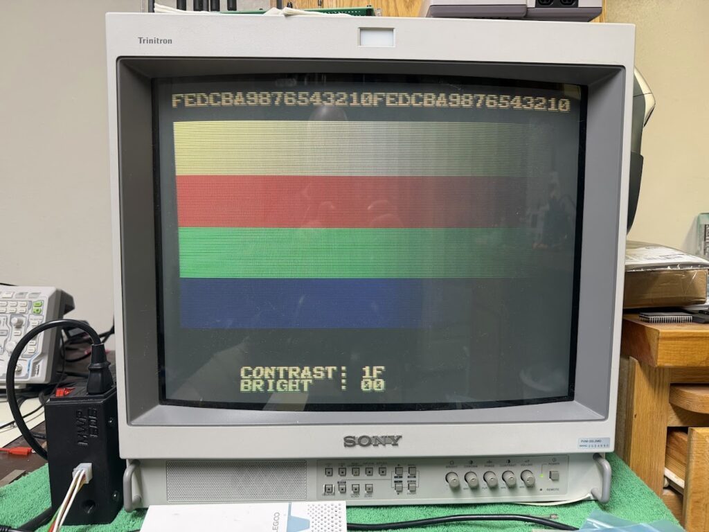
In for repair is a Cave CV-1000 PCB where the colors are displaying dim with a yellow tinge.
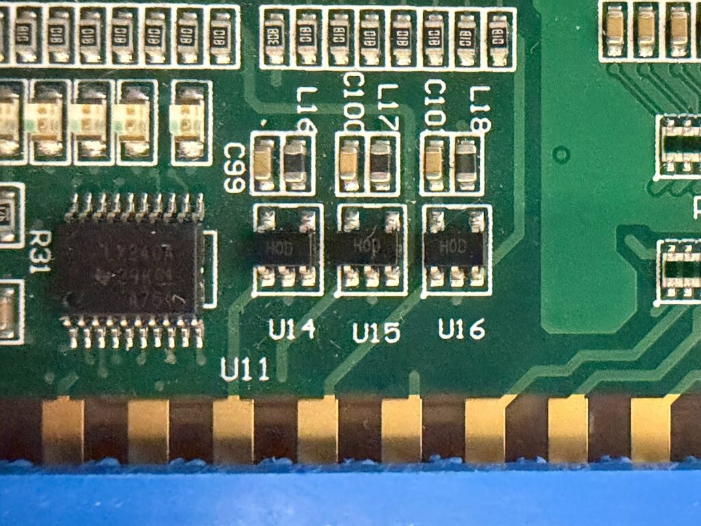
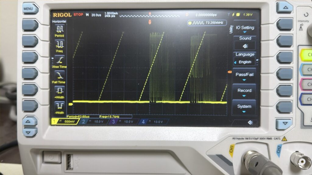
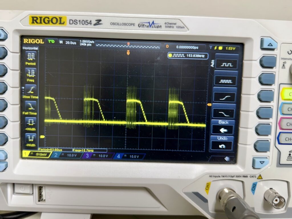
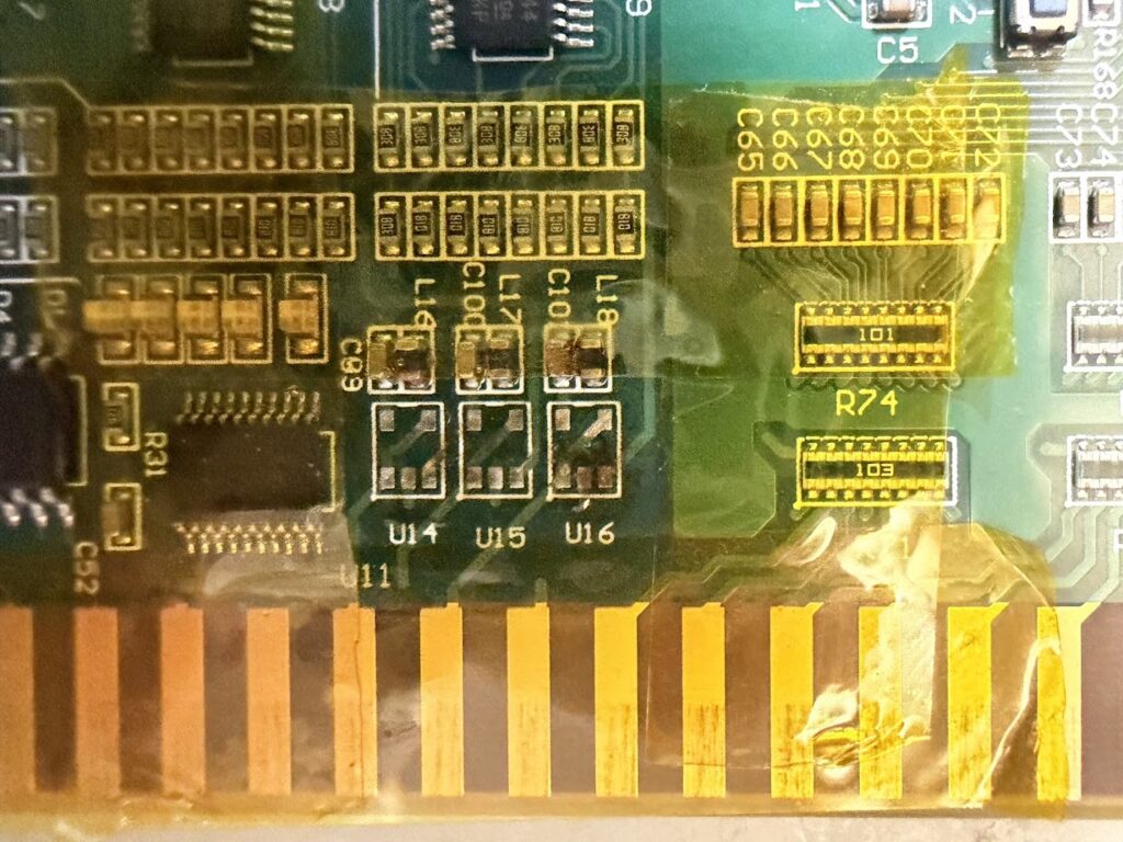
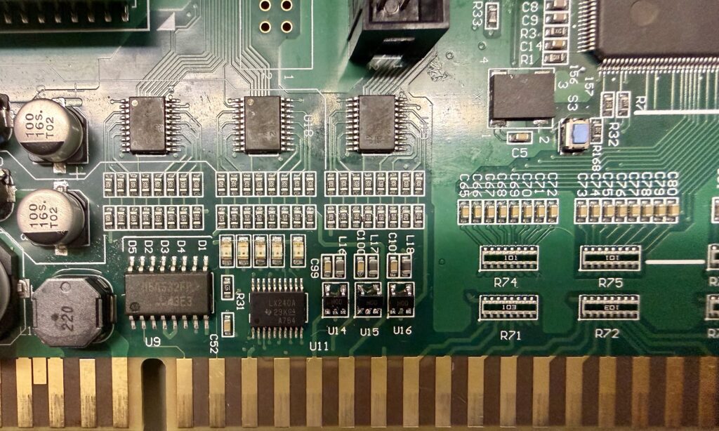
As per the PCB Encyclopedia, it is common for the three (U14=Red, U15=Green, U16=Blue) color amplifiers to fail on these boards. Testing the amplified output line of each amp on the oscilloscope quickly revealed a faulty Blue color amp.
Healthy color amp signalUnhealthy color amp signal
The part number for the color amps is AD8061. I ordered in replacements from DigiKey. Even though only the Blue color amp was obviously bad, I replaced all three amps to ensure that they’d all be fresh and matched with each other.
I masked off the color amps with kapton tape, and used Chip Quik to remove the old components.I used my smallest soldering tip with plenty of flux to install the new parts.
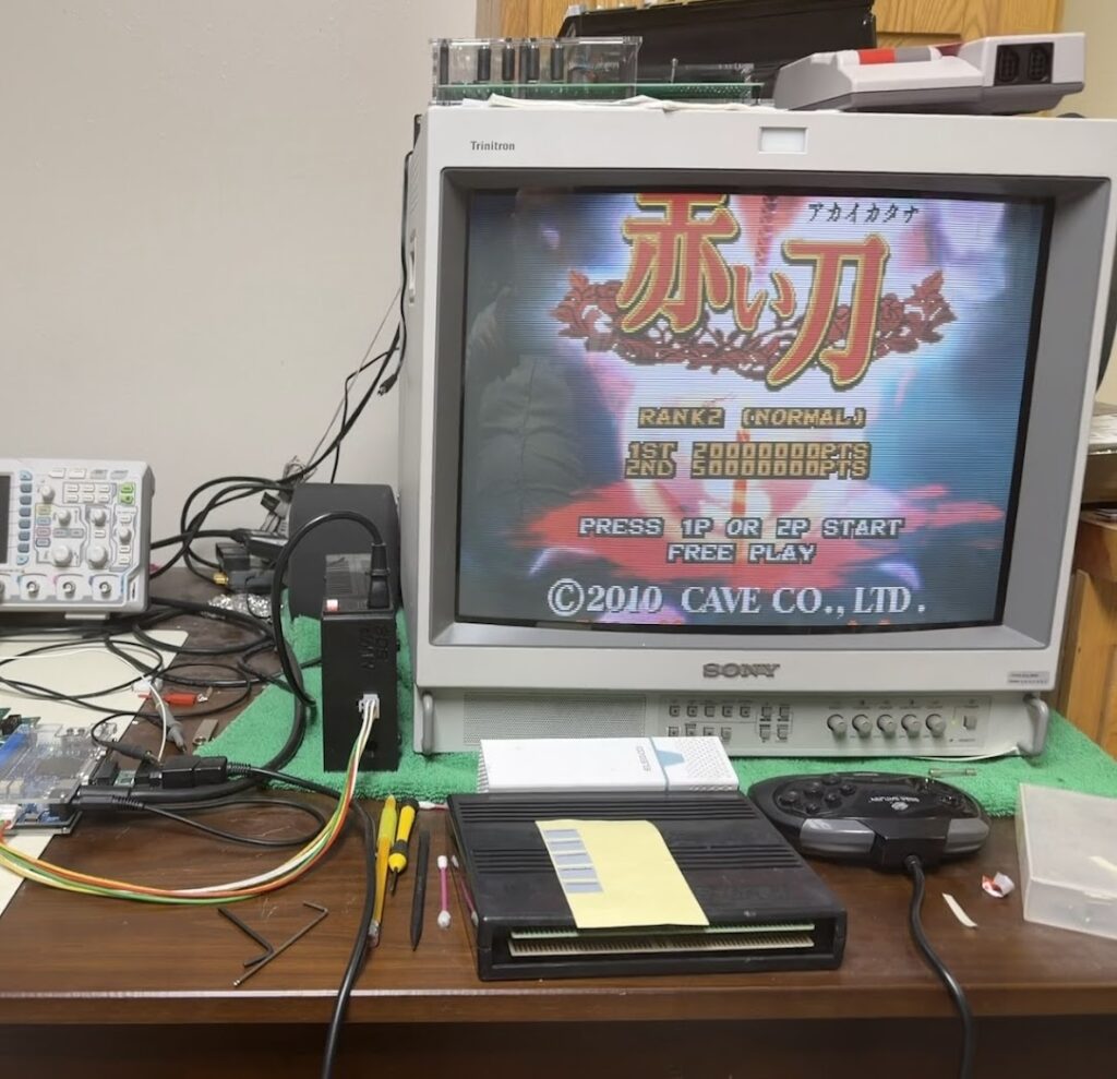
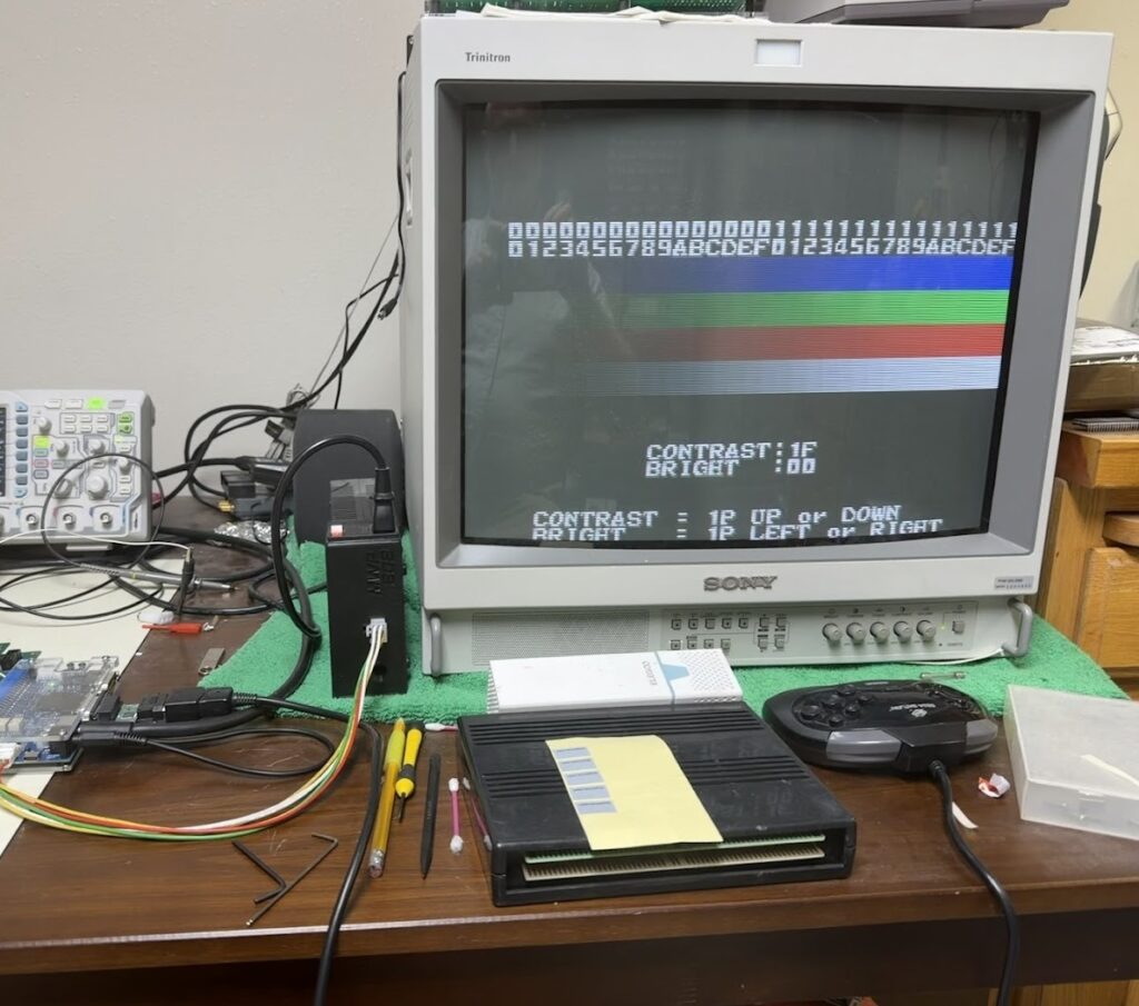
After confirming the new parts were connected without solder bridges with my multimeter, I powered on the board and was greeted by a sharp, colorful tinge-free display.
Another successful repair. I was nervous working on this one because of how spendy these boards are! 😀
PCB Repair LogsComments Off on Fighting Layer – Namco System 12 Repair
Apr132026
Kudos to Hammy for his expert advice of all things Namco System 11/12 for tutoring me on diagnosing this board.
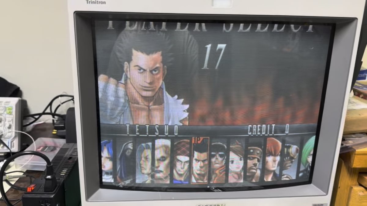
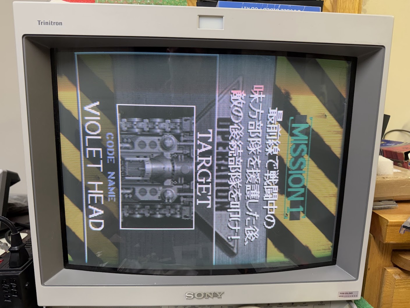
In for repair is a Namco System 12 boardset with the Arika game Fighting Layer.
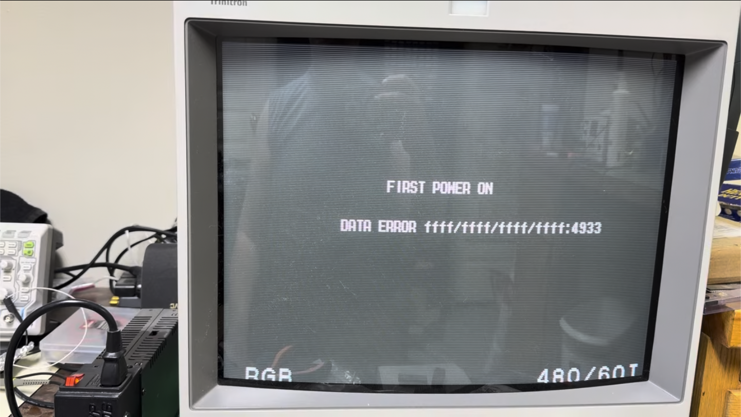
At startup, the board would display the error “FIRST POWER ON – DATA ERROR ffff/ffff/ffff/ffff:4933”. However, after displaying that error, the game would proceed to the title screen and play normally.
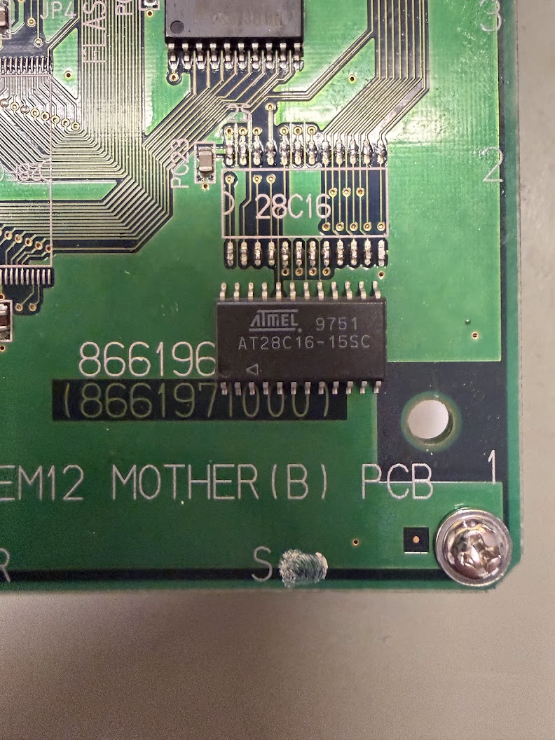
I assumed that the game was attempting to read corrupt bookkeeping info and stats from the onboard Atmel EEPROM chip located in the lower-right corner of the mainboard. Clearing the EEPROM contents in the Service Menu didn’t resolve the error though.
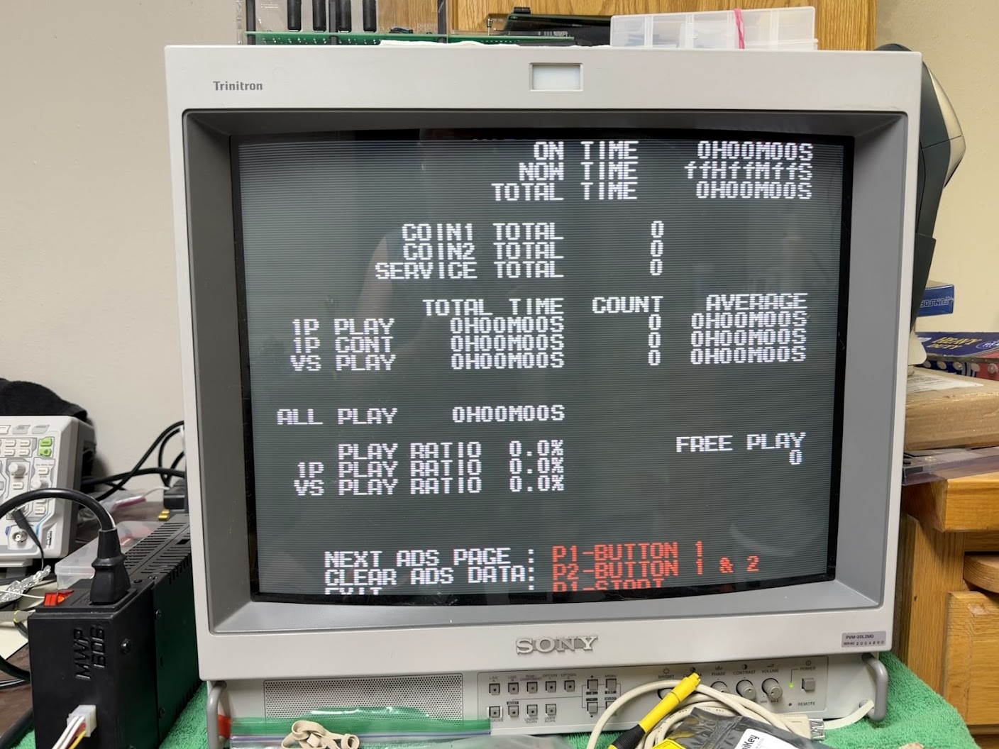
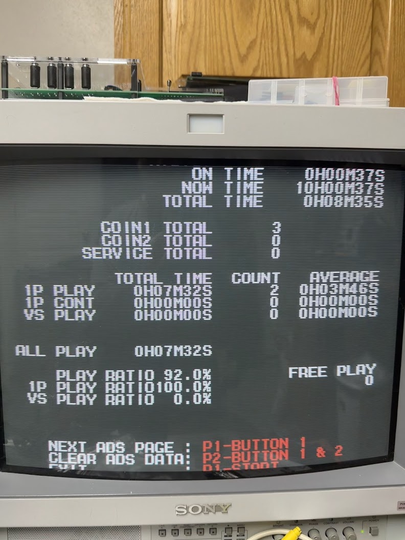
Notice how the “Now Time” counter in the upper-right corner didn’t reset to zeroes and shows all “ff”? We’ll be revisiting that shortly…
I’d been messaging online with Hammy – the resident Namco System 11/12 expert – and on his recommendation I swapped in a replacement Atmel AT28C16-15SC EEPROM.
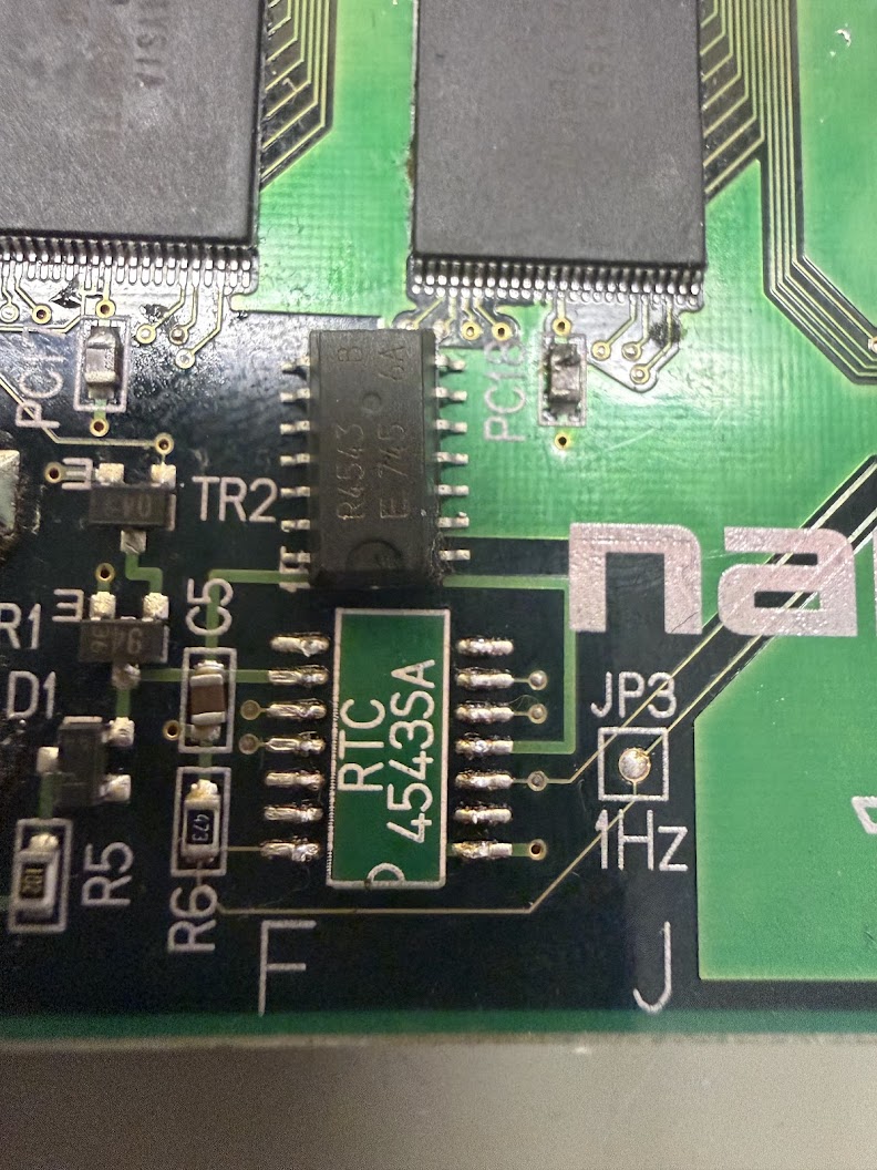
Unfortunately, the startup error and corrupt “Now Time” stayed the same. On Hammy’s recommendation, I next replaced the Epson R4543 RTC chip that’s adjacent to the battery in the lower middle edge of the mainboard.
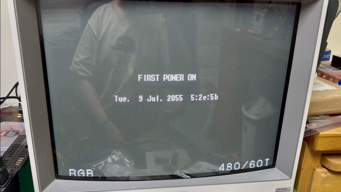
That was the culprit. This time when I powered on the board, it still said “FIRST POWER ON” but with a date far in the future rather than a DATA EROR.
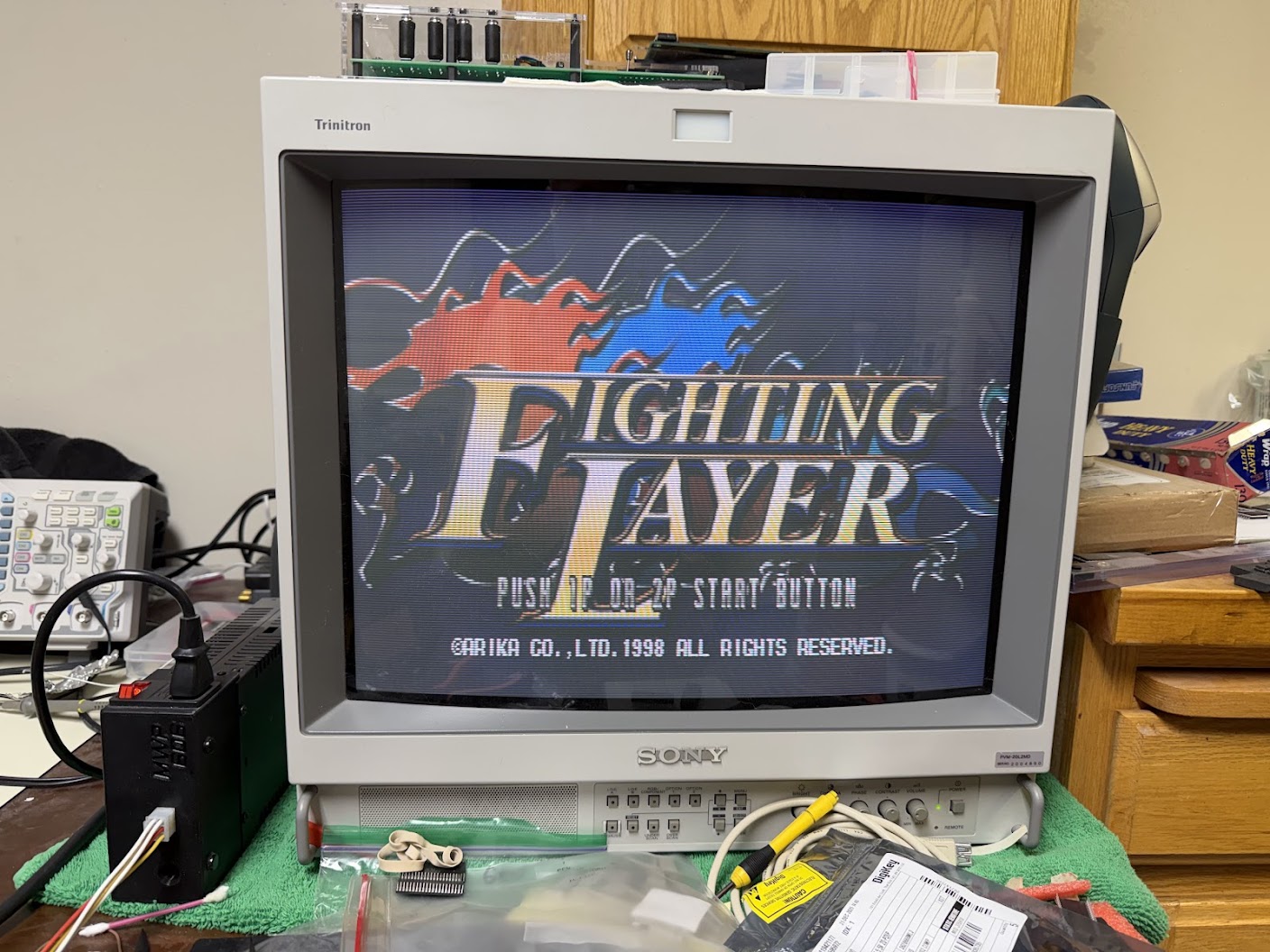
The “Now Time” in the Service Menu was now ticking up from 00H00M00S and when I checked the board again the next day, it was still reading time correctly. The board also booted directly into the game without any error messages. I played a few rounds and confirmed that the bookkeeping info and stats were saving correctly into the EEPROM as well.
So that’s another successful repair, but with one remaining mystery – how do I set the clock? I checked all through the Service Menus and also checked the written Operating Manual (RTFM!) that was shipped to arcade operators with the board back in the day and could not find the answer. Oh well. Fortunately you don’t need to know the time of day to have a good brawl!
PCB Repair LogsComments Off on Golden Axe II – Sega System 32 Repair
Feb262026
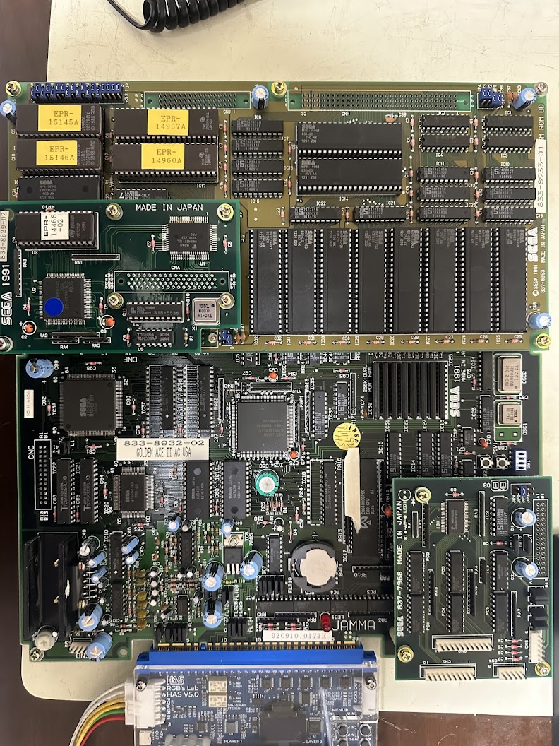
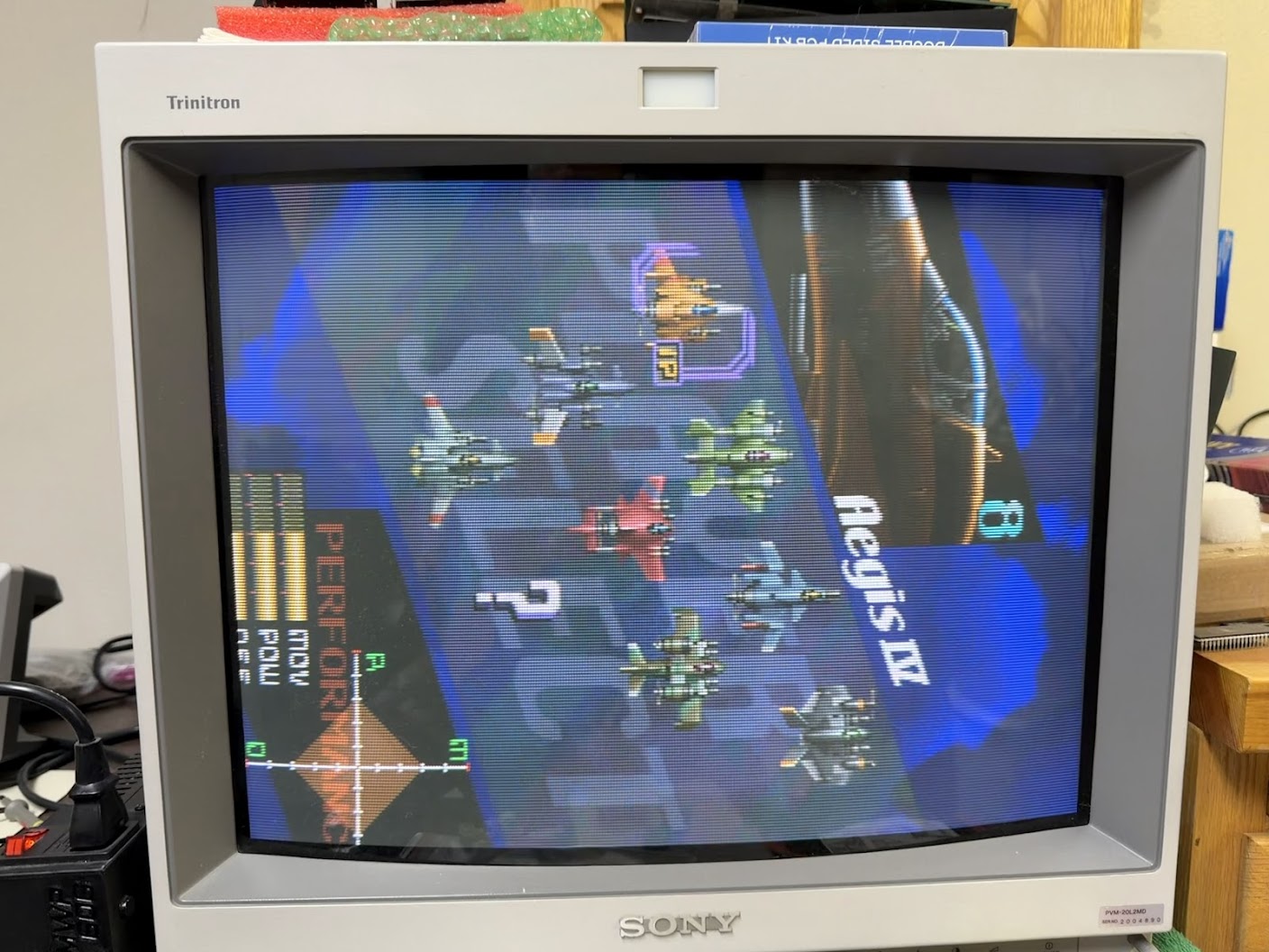
In for repair is a Sega Golden Axe II Revenge of Death Adder boardset. The board set consists of a large mainboard that handles all the logic processing, a daughterboard with the game data ROMs and another daughterboard that handles inputs for Player 3 and Player 4.
Although the boardset is in clean physical condition, it doesn’t boot up.
The first question with any Sega System 16, 18 or 32 game board that won’t boot up is “Has it suicided?” All three platforms used encrypted code on the CPU ROMs and a protection mechanism to decrypt the code before it runs on the Main CPU. If the protection mechanism fails then the Main CPU hangs waiting for code it can run. Sometimes the protection mechanism is battery-powered, and when the battery dies then the decryption mechanism permanently breaks – hence the term “suicide”.
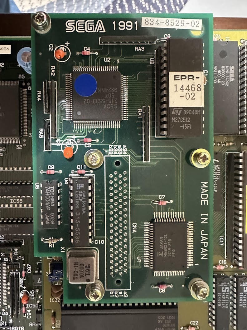
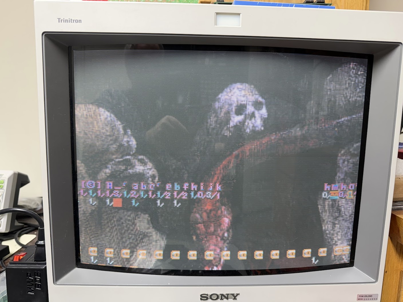
In the case of Golden Axe II, the protection mechanism is this small daughterboard sitting on top of the ROM board.
This protection board is a mini-computer by itself. The Sega 315-5533-02 is a relabeled NEC V25 CPU running at 10 mhz that executes its code from the single onboard EPROM and uses the Fujitsu RAM for processing the decryption algorithms. Here, it’s possible for either the onboard EPROM to become corrupted or the Fujitsu RAM to fail, resulting in the decryption CPU crashing and the Main CPU then hanging up waiting for incoming code it can run. At least there’s not a battery here to worry about…
Fortunately, I had a quick and easy method to determine if this Golden Axe II ROM board had suicided. I have my own fully-functional Golden Axe II board set, so I swapped the project’s ROM board over to my personal main board and powered up.
The game booted up and played perfectly. Therefore the ROM board hasn’t suicided and the problem is with the System 32 main board.
I hadn’t worked on a System 32 main board before, so I started performing some research. Specifically, I wanted to know:
Are schematics available for this hardware?
Are there repair logs of other technicians resolving similar issues with this hardware?
As far as schematics go, Nemesis has scanned and shared them. In order to aid SEO, I also mirrored them here. As far as repair logs go, The Guru has logs on several similar System 32 repairs. Here are some key discoveries I made from Guru’s writeups about Sega System 32 hardware when the main board doesn’t boot up:
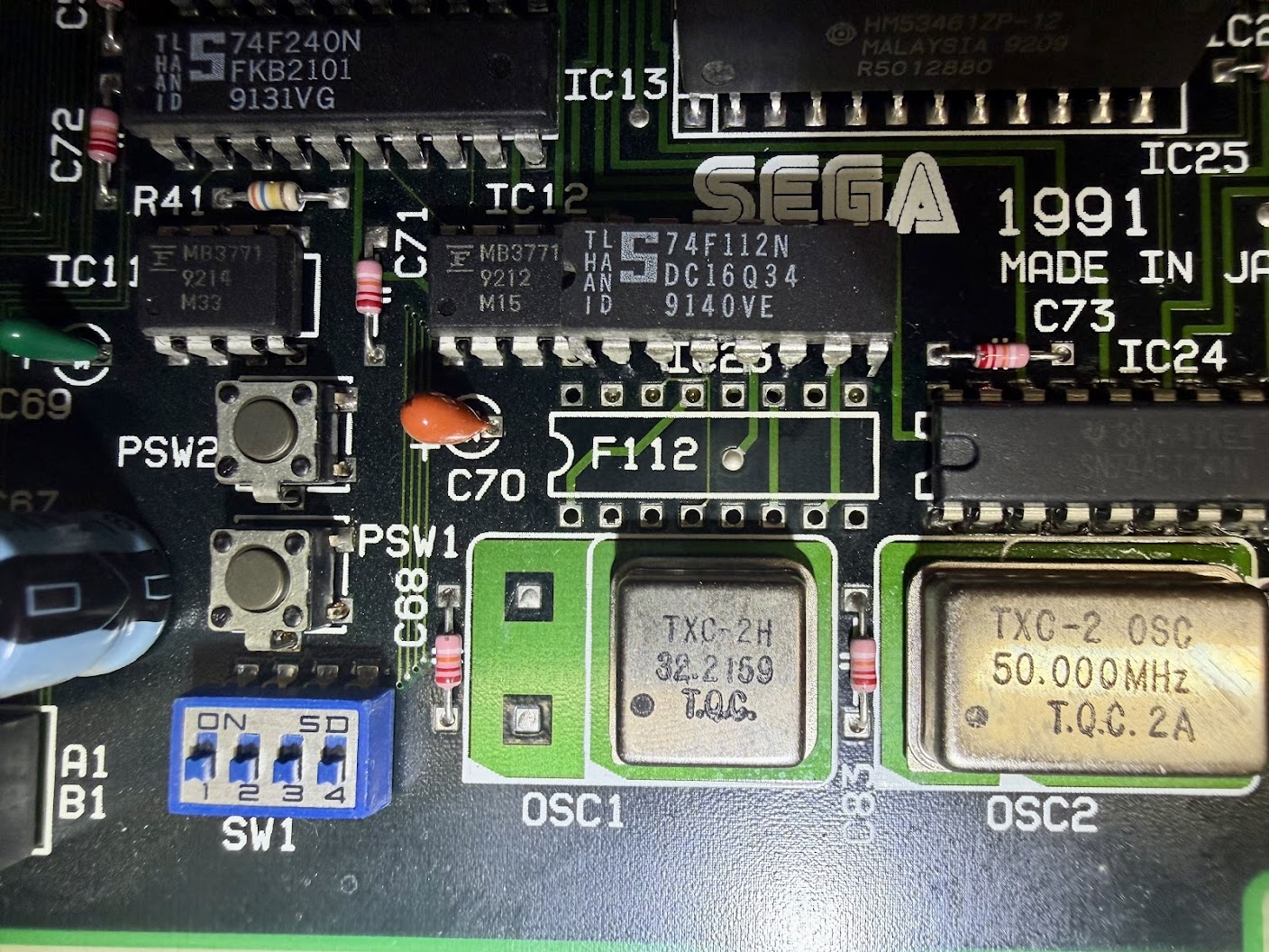
Reset signals originate at the TTL logic chips located at IC11 and IC12.
Clock signals originate at the two oscillators at the bottom-middle of the board and are distributed around the board by a handful of TTL logic chips (IC23, IC24, IC34, IC39, IC52, IC53).
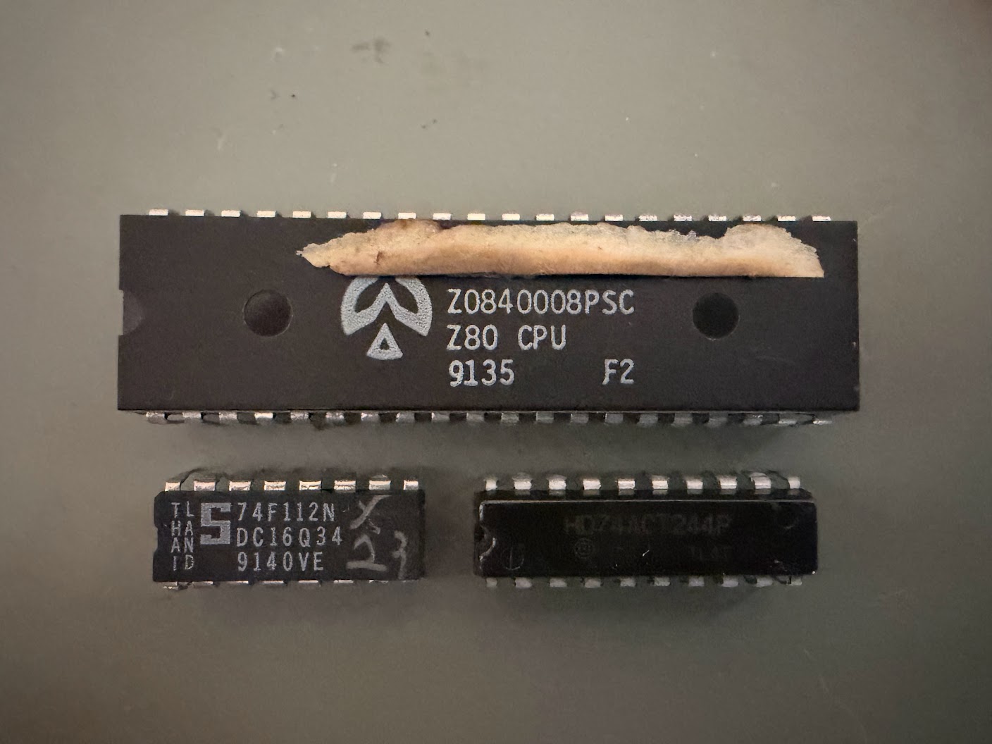
The game will not boot if the NEC V60 Main CPU, Zilog Z80 Sound CPU or 315-5296 custom are nonfunctional.
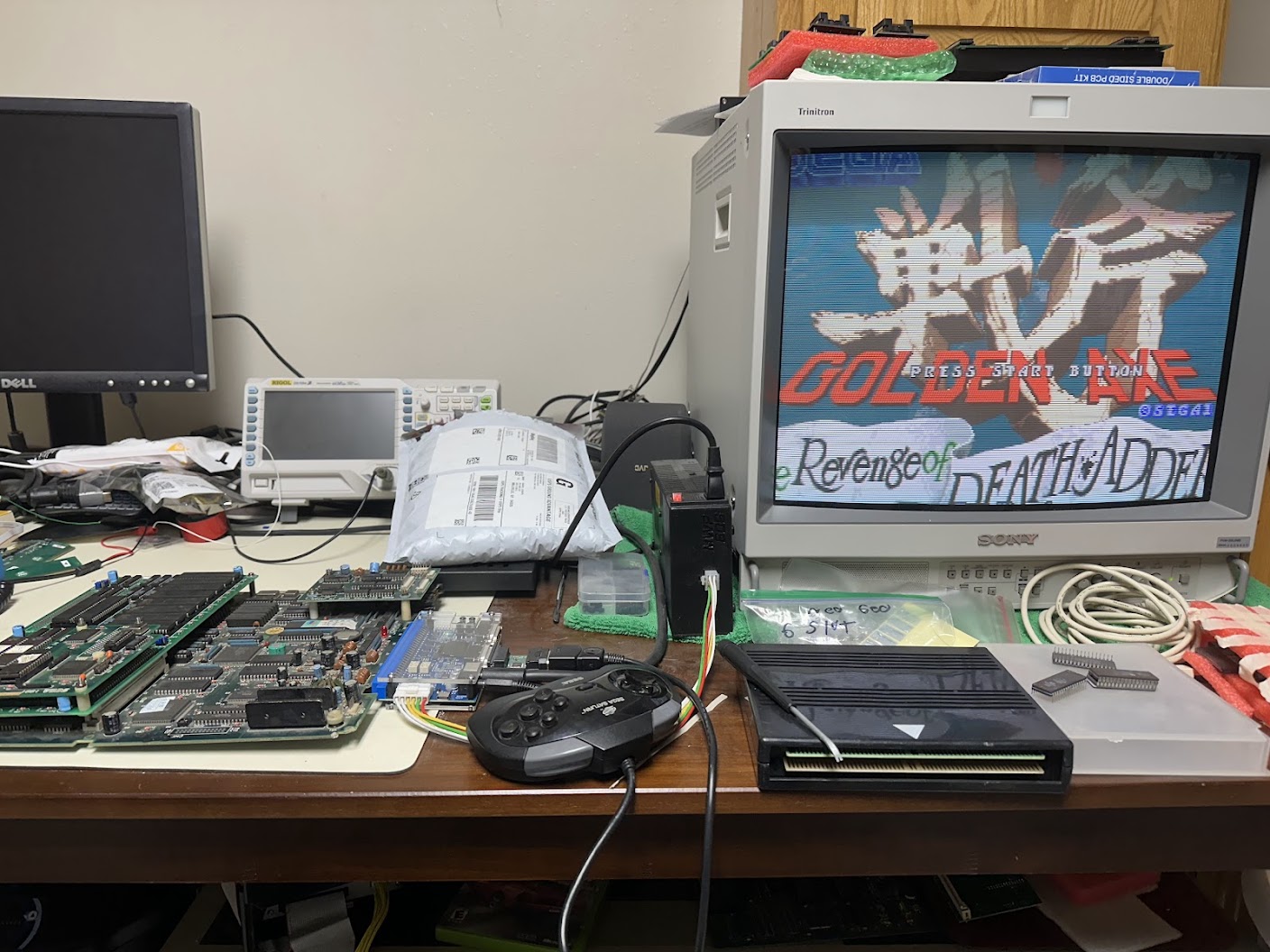
Time to dig in. I started with checking the Reset signals. The Main CPU, Sound CPU, and some of the other components on the board need to be Reset when the board starts up. There is also a “watchdog” circuit which will trigger the Reset lines and reboot the game if the watchdog detects that the game has frozen. On a logic probe or oscilloscope, the Reset pin on a CPU should initially read High at powerup, go Low briefly as the Reset circuit triggers, then return to High.
I probed the NEC V60 Main CPU Pin 52, Z80 Sound CPU Pin 26 and the outputs on the TTL logic chips at IC11 and IC12. They all showed that the Reset circuit was operating as expected.
V60 Main CPU Reset Line from the schematicsZ80 SoundCPU Reset Line from the schematics
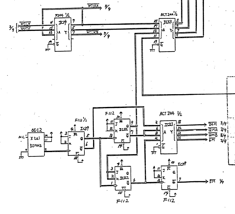
Next, I investigated the Clock signals. Think of the Clock as a “heartbeat” that drives the processing logic on the board and keeps everything in sync. Without appropriate Clock signals, the board won’t run.
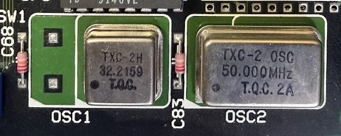
Clock signals originate from crystal oscillators. The Sega System 32 main board has two of them located in the bottom middle of the board – a 32.2169 mhz clock and a 50 mhz clock.
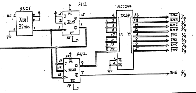
These clock signals are then distributed around the board and subdivided to lower speeds as needed by a variety of TTL logic chips. Here is the appropriate clock distribution circuits from the schematics.
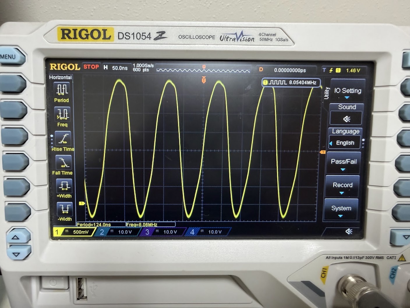
Many components need a clock signal, but I started by checking the clock input pin on the NEC V60 Main CPU first. The V60 Clock Input pin is Pin 13 and it showed the expected 16 mhz clock signal.
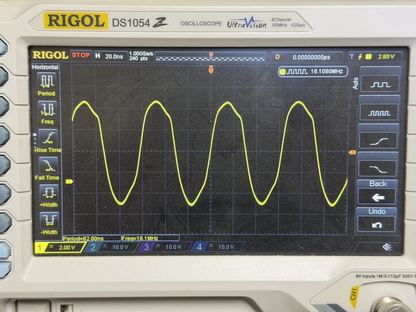
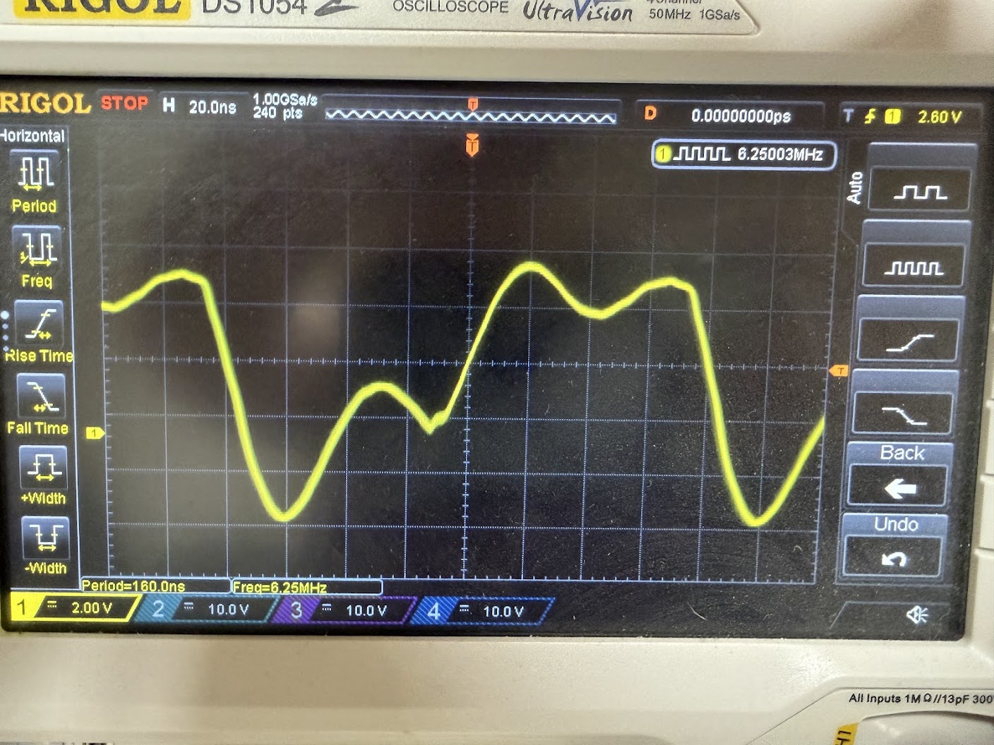
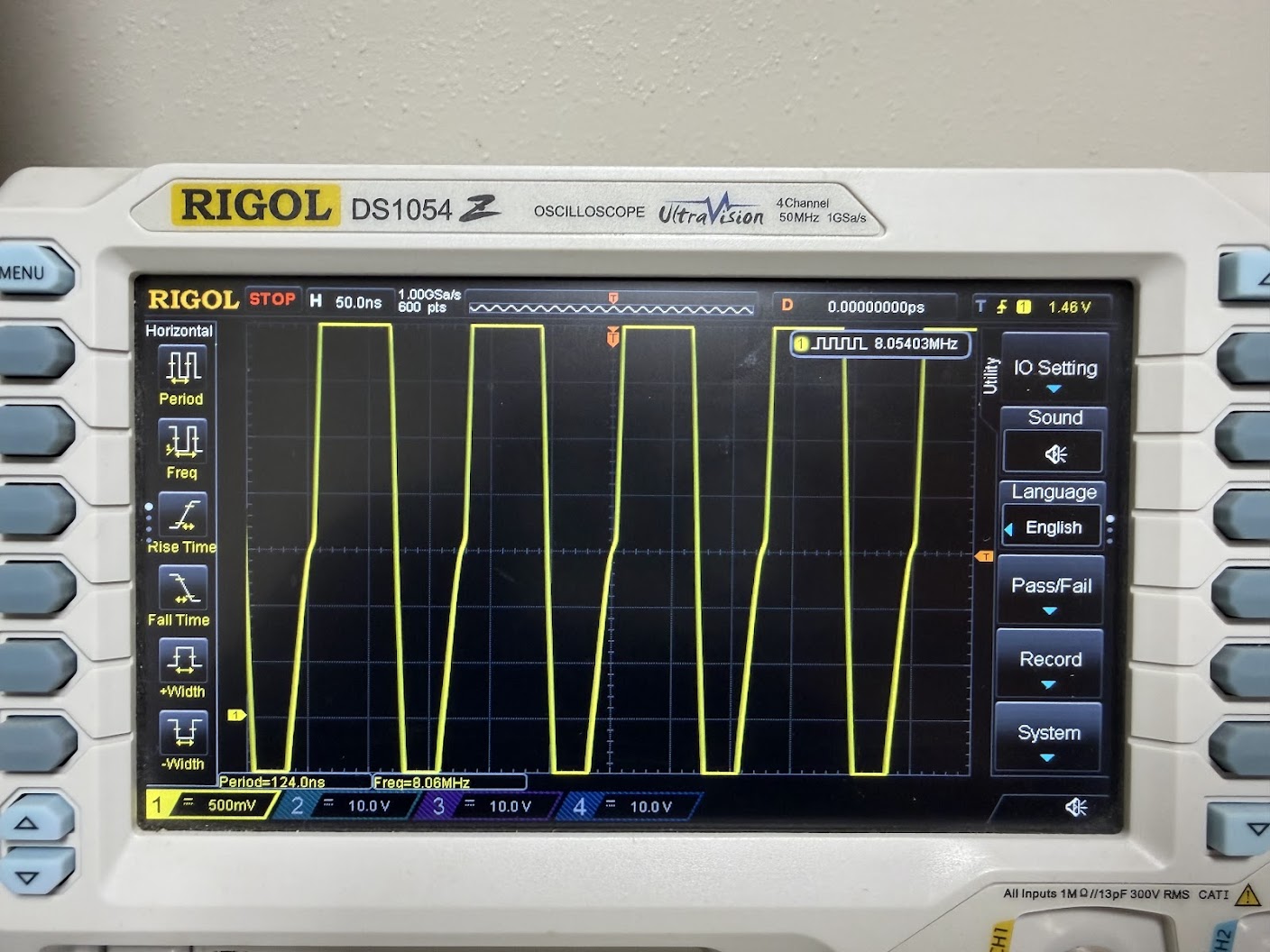
The Z80 Sound CPU clock input is Pin 6 and its signal looked awful.
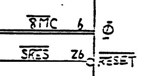
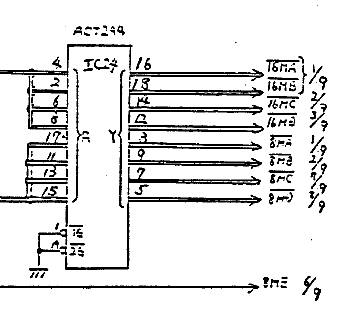
Time to check the TTL logic chips that feed the clock signal to the Z80. The Z80 clock signal line is labeled “8MC” on the schematics.
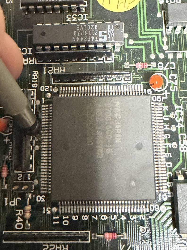
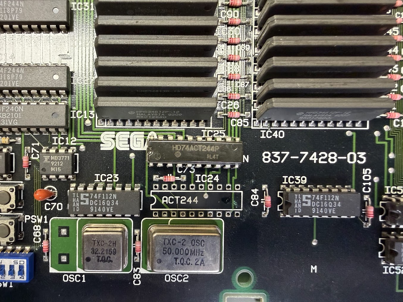
And the schematics show that 8MC is output from Pin 7 on a 74LSACT244 TTL chip located at IC24.
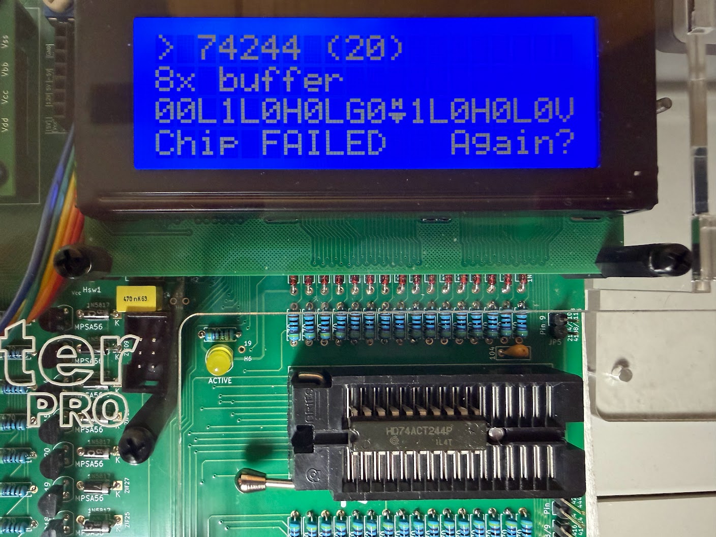
I desoldered IC24 from the board and it tested bad out-of-circuit in my logic chip tester.
Since clock signals are driven at a high speed, a standard 74LS244 replacement part won’t suffice. A standard 74LS244 can handle 10 – 15 ns signal switching. The ACT designation on both the schematics and board means that a faster ACT series chip capable of 1 -2 ns signal switching is needed. I had to order some in and for them to arrive.
Unfortunately, the replacement part didn’t fix the board – it still hung with a black screen at boot. I started probing around the other TTL parts in the clock distribution circuits, when to my surprise the board suddenly sprung to life!
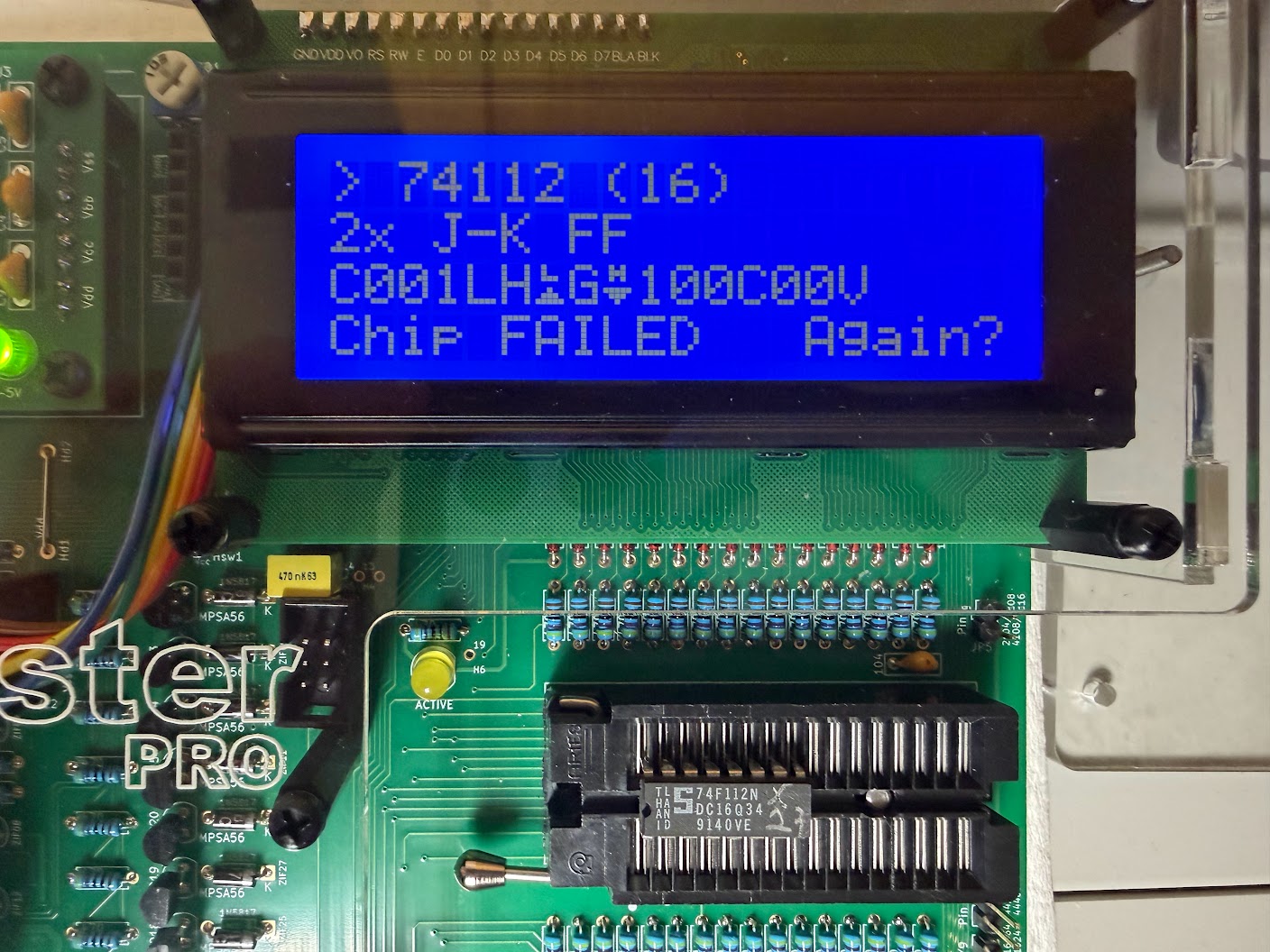
Sure, the sprites were garbled and there wasn’t any sound, but I was still pleased to see signs of life. This definitely hints at more problems in the clock distribution circuits. I found that probing IC23 is what would jumpstart the board, so I desoldered that part from the board, and sure enough it tested bad out of circuit.
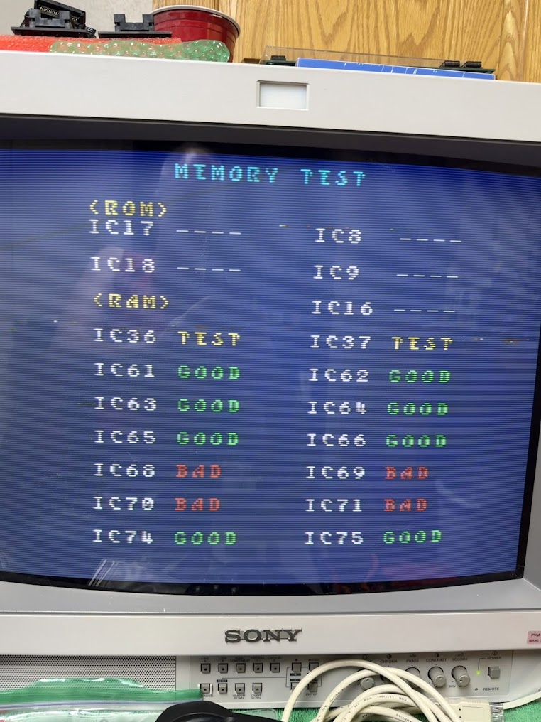
This part is a 74F112N and I had planned ahead and ordered replacements for these in at the same time as the ACT244s, so I was able to swap a fresh part in right away. However, it still didn’t completely solve the problem. The board would now boot up on its own with clean graphics, but not consistently. The sound also didn’t work, and the game would freeze up often. The self-diagnostic routine in the Service Menu marked four components as faulty and then froze when testing the ROMs.
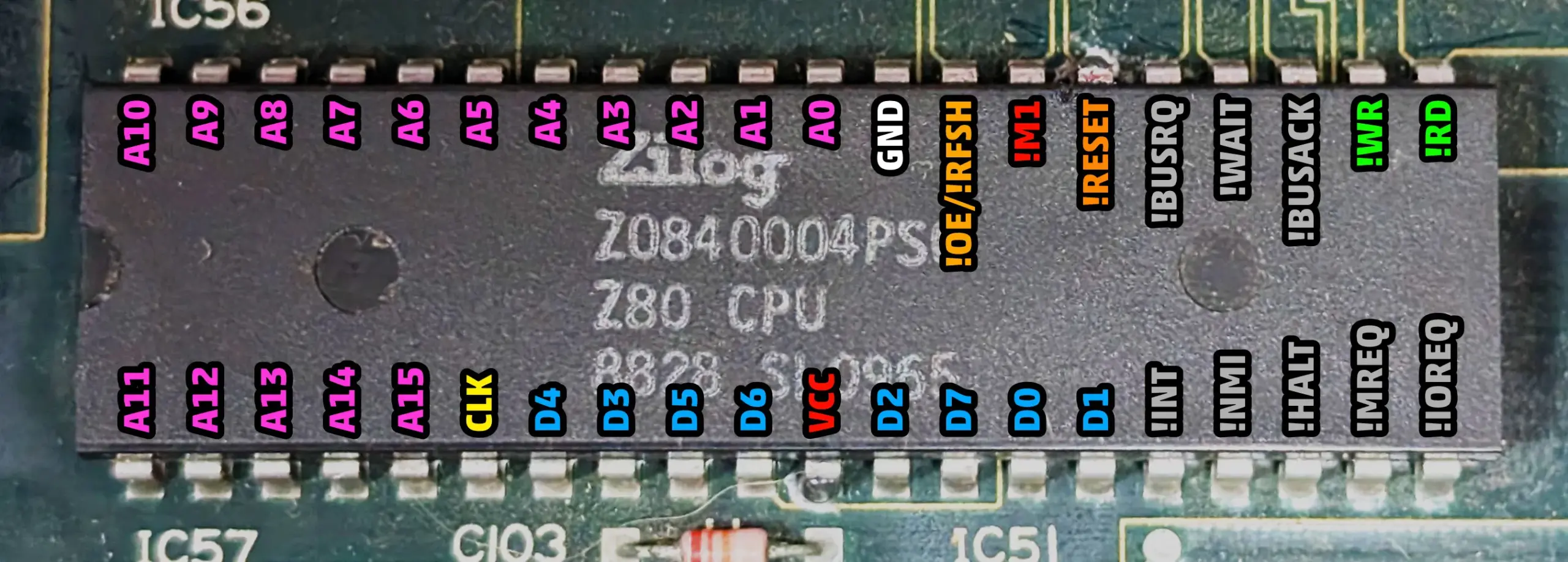
Since the sound wasn’t working, I decided to check the Z80 Sound CPU in detail for proper operation next.
In addition to the Clock and Reset signals I mentioned earlier, there is also the HALT signal on Pin 18 that will go High only if the Z80 software program triggers it to stop. It probed Low as expected.
Pin 27 is M1 and it starts High and toggles Low when fetching an opcode from memory at the beginning of every machine instruction in the software program. The M1 signal on this Z80 probed as holding High continually so the CPU was not processing instructions – very suspicious.
Next, I checked the WAIT signal on Pin 24. If it is holding Low then another component on the board is triggering the Z80 CPU to stop. It probed as holding High, so nothing else was triggering the Z80 to wait.
Then, I checked the BUSRQ (Bus Request) signal on Pin 25. If it reads Low, that means that another peripheral on the board (such as a DMA controller) has asked the Z80 to release the bus so shared resources (such as memory) can be accessed. The Z80 triggers the BUSAK (Bus Acknowledge) signal after it’s released the bus so that the requesting peripheral knows it can proceed with its operations. The requesting peripheral would then set BUSRQ back to High again when it completed its work and was ready for the Z80 to take back the bus and resume operation. In this case, the BUSRQ signal showed High briefly at power on, then went Low and held there. This meant that the Z80 was receiving a signal to release the bus but then never received a signal to “wake back up” again. Suspicious!
Finally, I checked the BUSAK signal on Pin 23 and finally found the smoking gun. BUSAK is only supposed to trigger after a BUSRQ signal, but on this Z80 the BUSAK was triggering continuously – at exactly the same frequency as the Z80’s 8 mhz Clock signal no less!
Unexpected 8 mhz signal pulsing on the Z80 Sound CPU’s BUSAK pinThe Z80 Sound CPU’s 8 mhz Clock signal
This confirmed that the Z80 Sound CPU had failed internally in such a way that the BUSAK line was “echoing” the Clock signal. That was likely confusing all the other components on the board that tied to it!
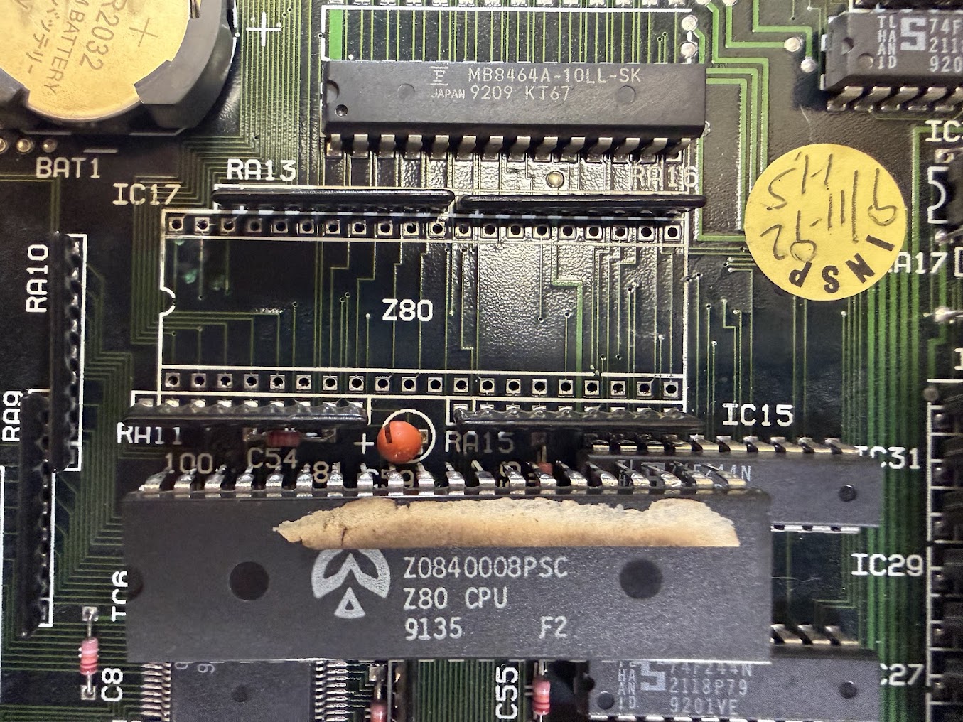
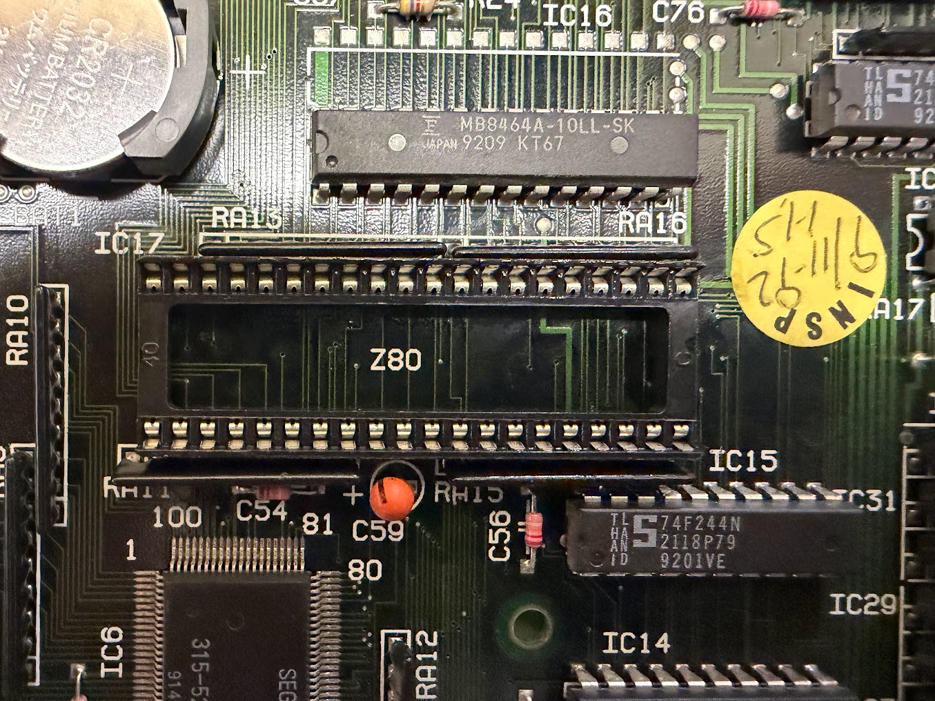
I desoldered the Z80 CPU, installed a 40 pin socket, and swapped in a replacement 8 mhz Z80 CPU.
Happily this time when powering on, the board functioned perfectly! Sound was present, the game didn’t freeze up, and the self-diagnostics passed with flying colors!
For good measure, I played through the entire game successfully, and left the game running overnight. There were no freezes and the game continued working perfectly. A successful repair!
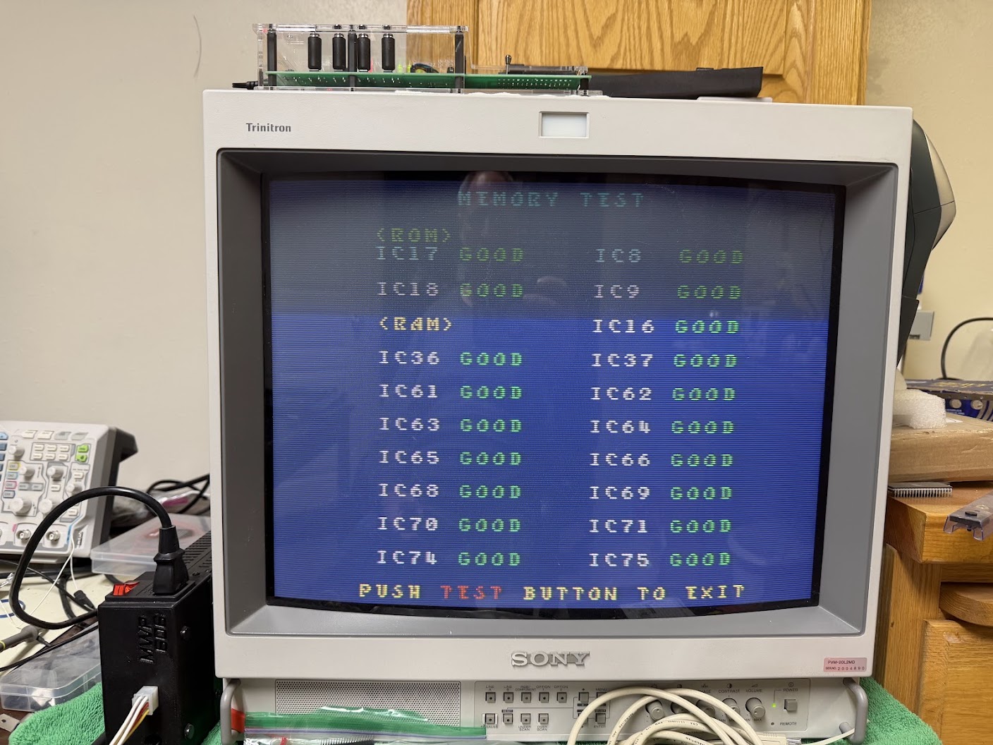
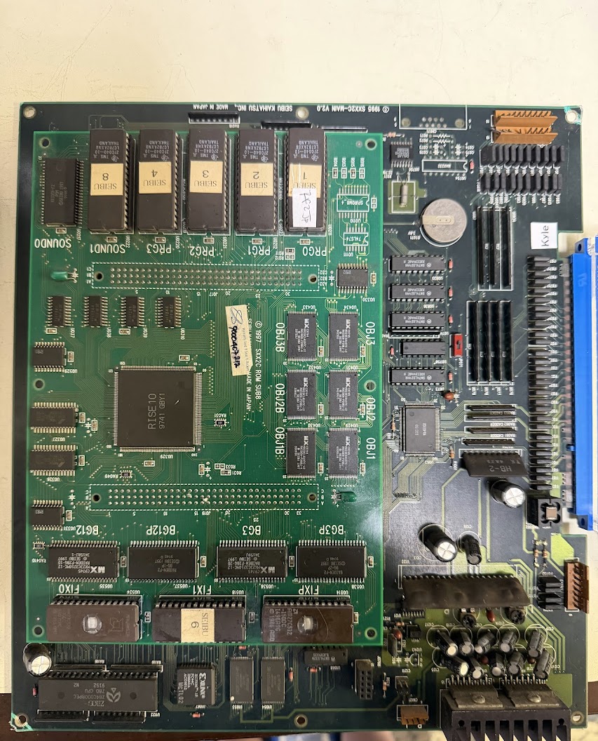
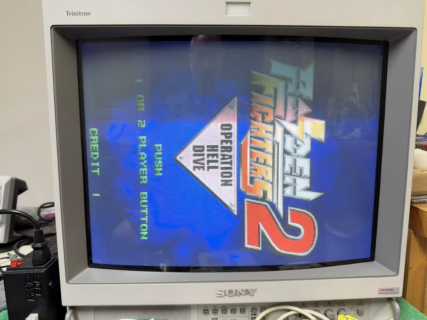
In for repair is a Seibu Kaihatsu SPI mainboard (V2.0 Revision) and a Raiden Fighters 2 game cartridge.
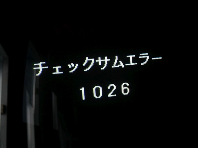
The SPI mainboard wouldn’t boot – on powerup, it would display a generic “Checksum Error” message.
This is a common problem with the SPI platform. The SPI mainboard and game carts are region coded. If the cart region doesn’t match the mainboard region then you’ll see this error. Additionally, when a game cartridge is accepted, portions of it are flashed to chips on the mainboard. If something goes wrong during the flash process, the mainboard’s region code can be lost, causing it to no longer work with any game.
Happily, Trap15 created a tool called SPI Revive that can be used to write a new region code onto an SPI mainboard. I connected my SPI Revive cartridge, and it shows that the region code for this board is “zero” meaning that it was indeed bricked. I told SPI Revive to write the Japan region code to the board, which it did successfully.
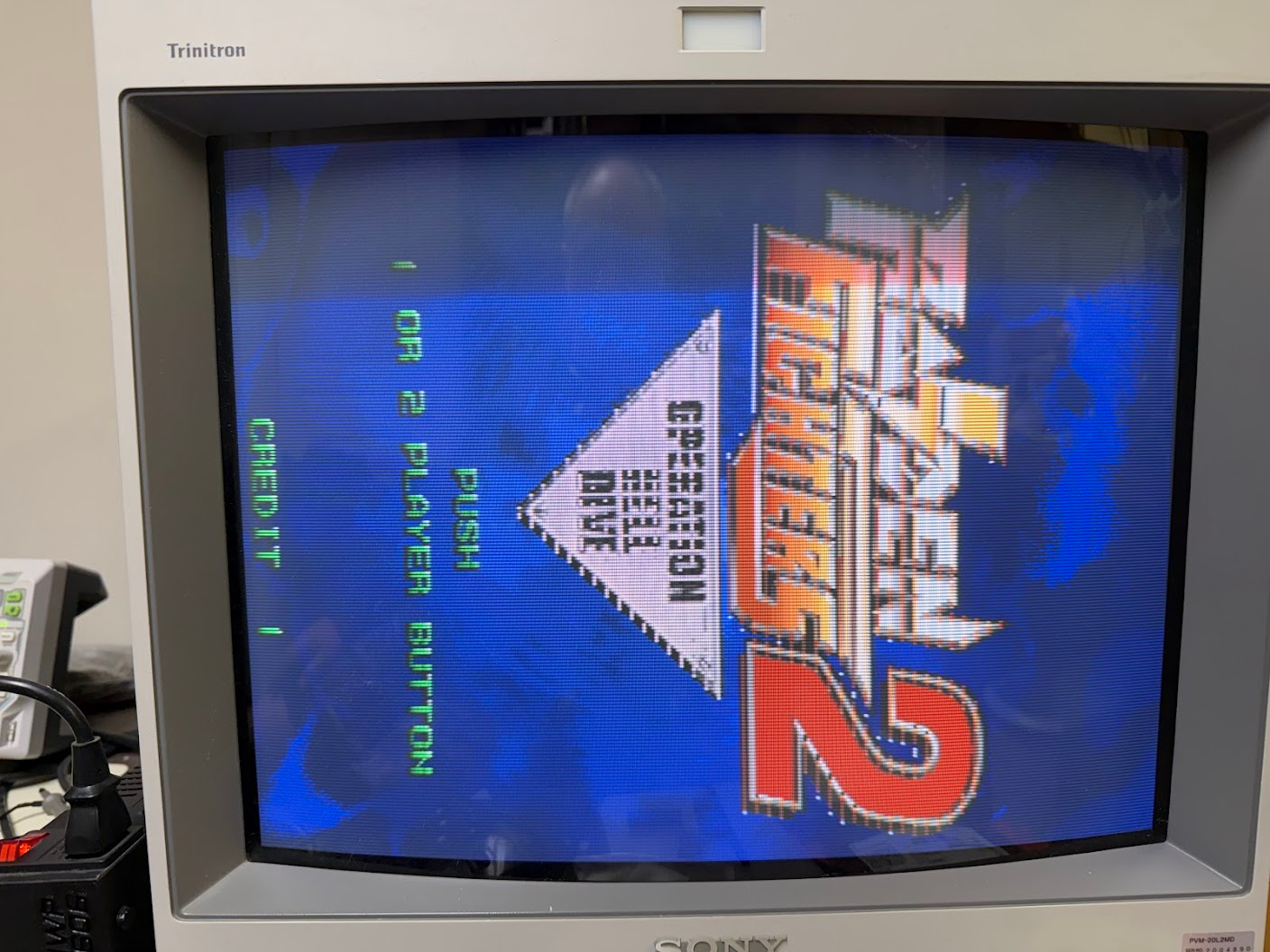
After reconnecting the Raiden Fighters 2 cart, the board started up successfully, flashed itself to the mainboard successfully, and then prompted to restart. After restarting, the game boots up and runs fine, but with “jailbar” lines of corruption running through the sprites.
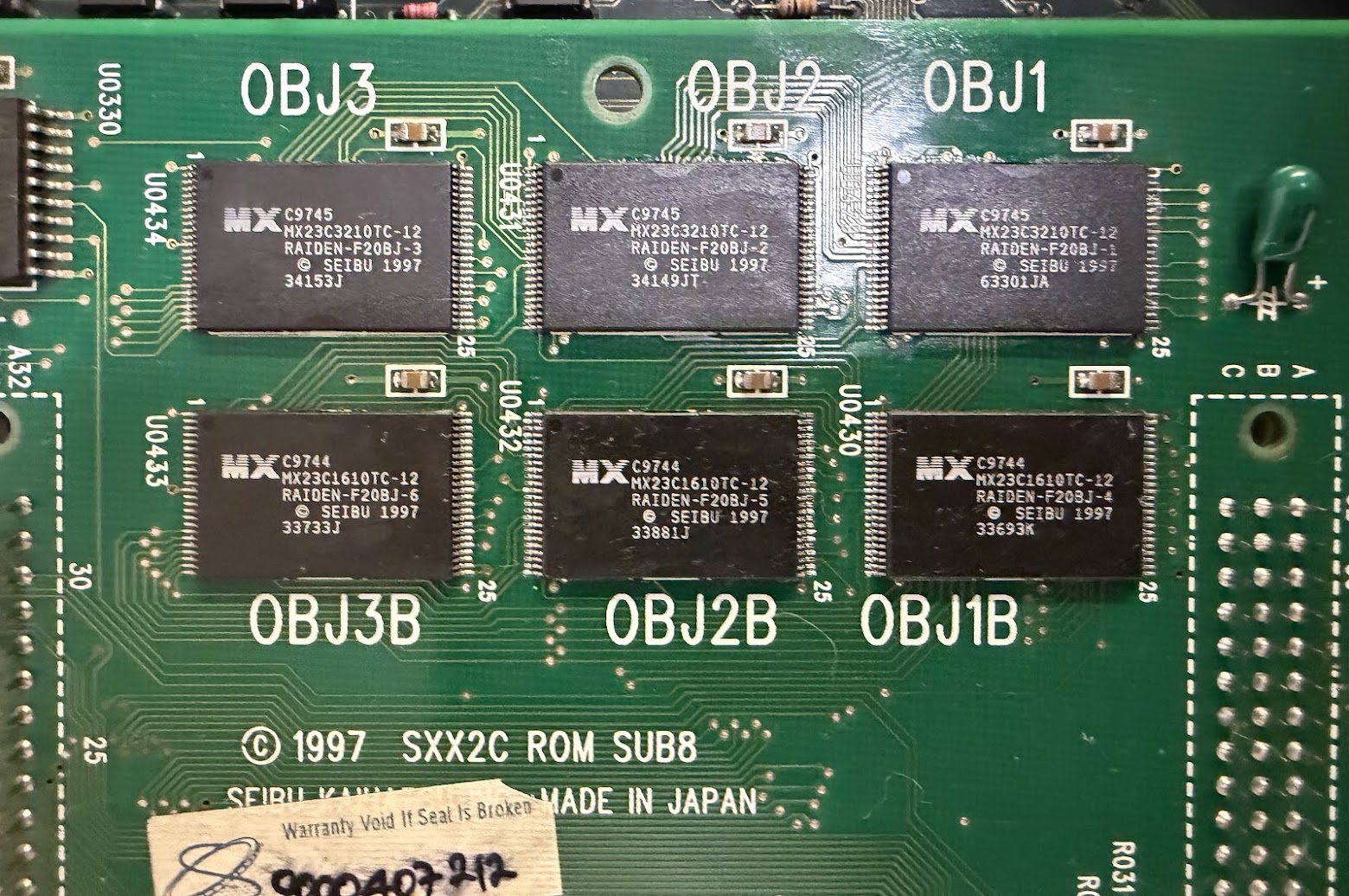
This is another common issue with game cartridges on this platform. There are several SMD ROMs and a large SMD custom chip. Not much solder was used at the factory and over time, some of the chip legs can detach from their solder pads, breaking the connection.
One way to test for this problem is to press on various chips on the PCB and watch the screen to see if the graphics change. I used a plastic spudger and noticed the jail bars would flicker when I used it to press on ROM chips in the OBJ section. I reflowed the solder on them.
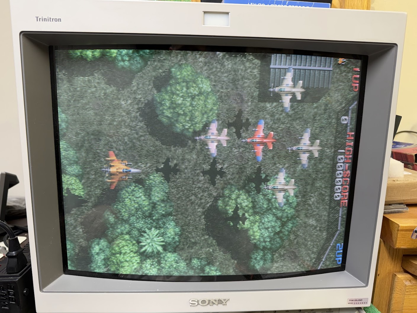
Afterward, the game boots up and runs fine with crisp, clear graphics and sound. The final touch is applying reflective stickers to cover the exposed windows on the two EPROMs missing them on the game cart. A successful repair!
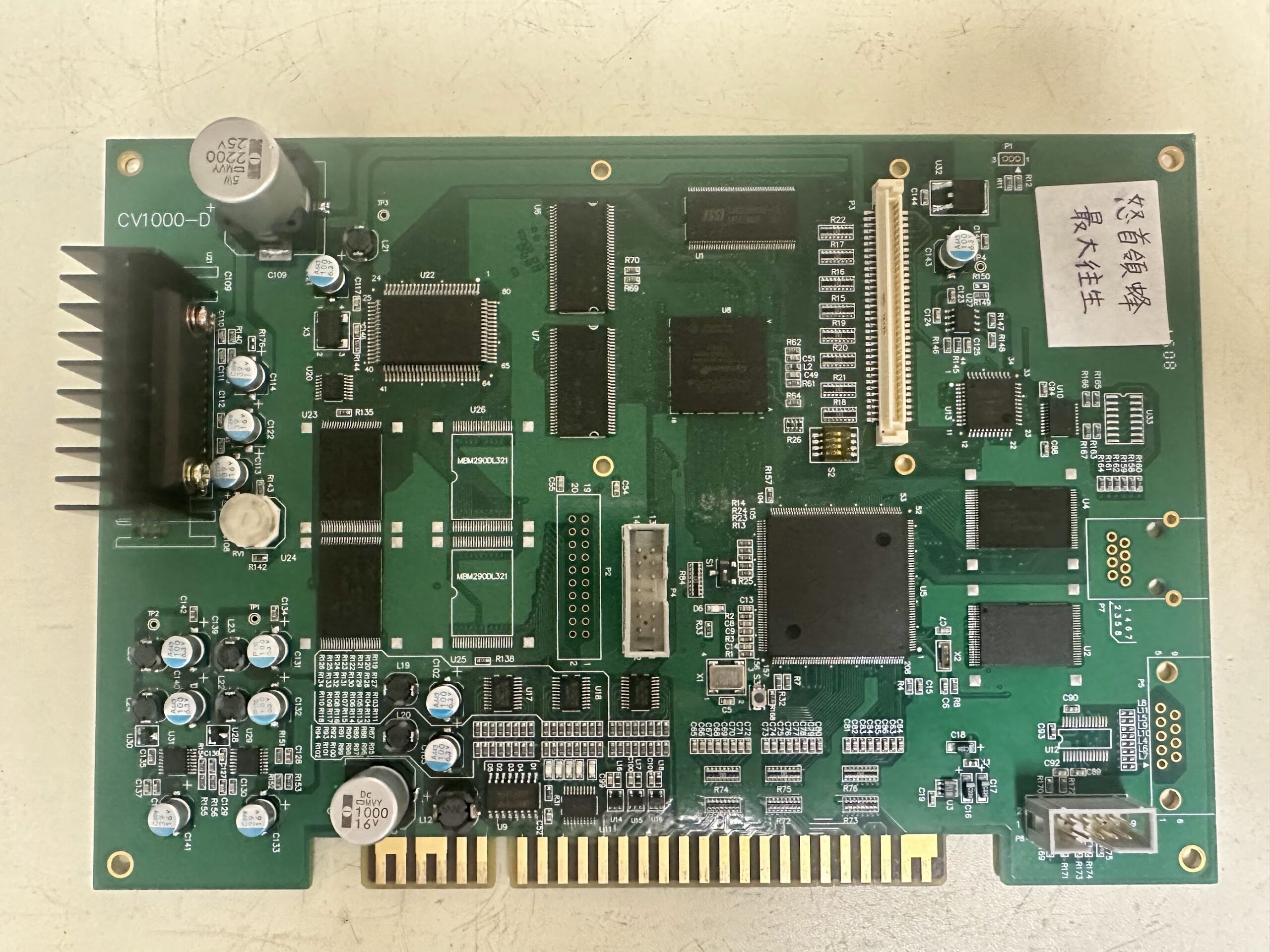
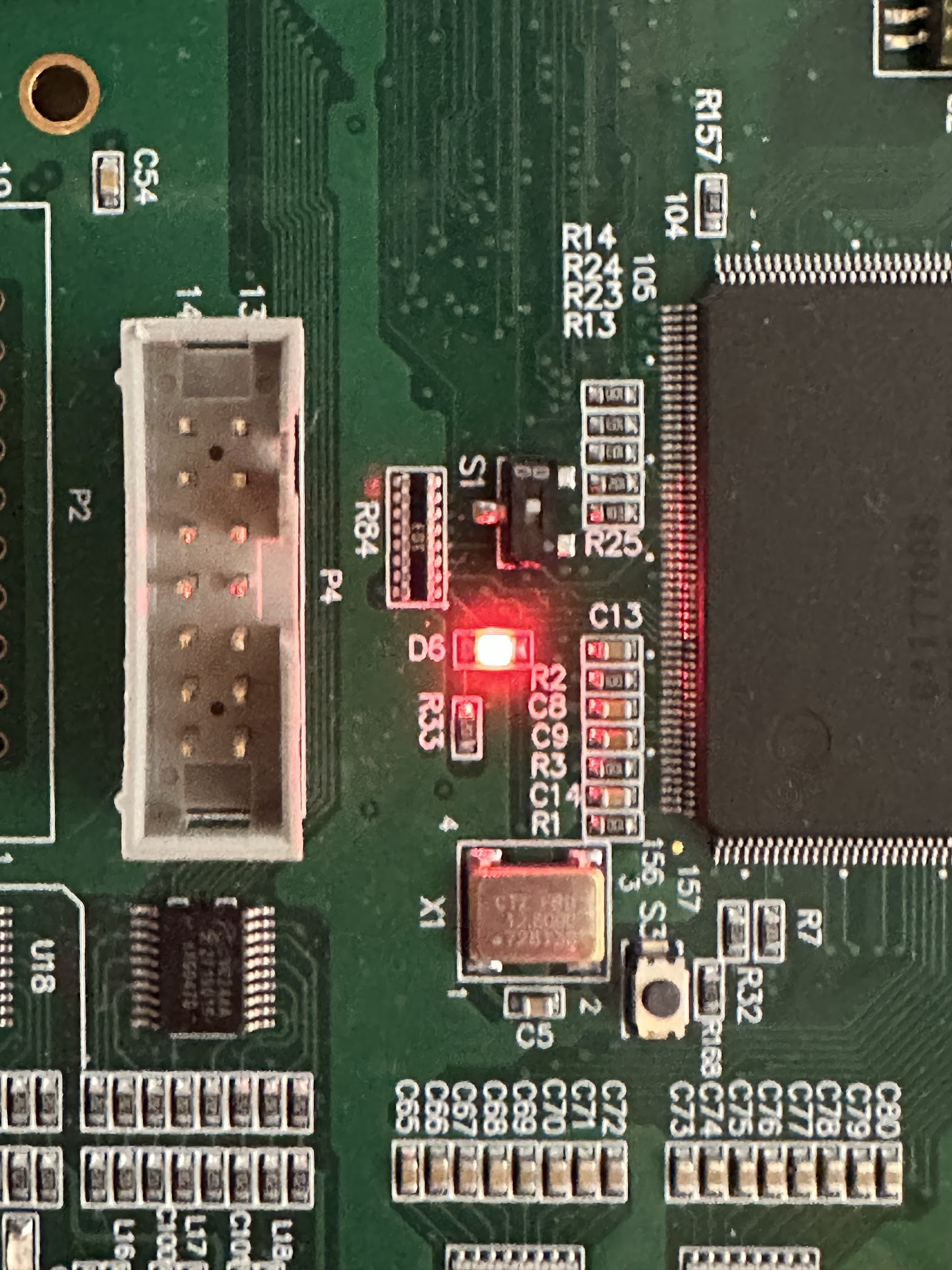
In for repair was DoDonPachi Saidaioujou, a Cave shoot-em-up running on a CV1000-D board. This board is one of the recent reproduction bootlegs that’s distinguishable from an original by having gold-plated JAMMA fingers rather than tin-plated.
The board would not boot up at all and a D6 LED would light up.
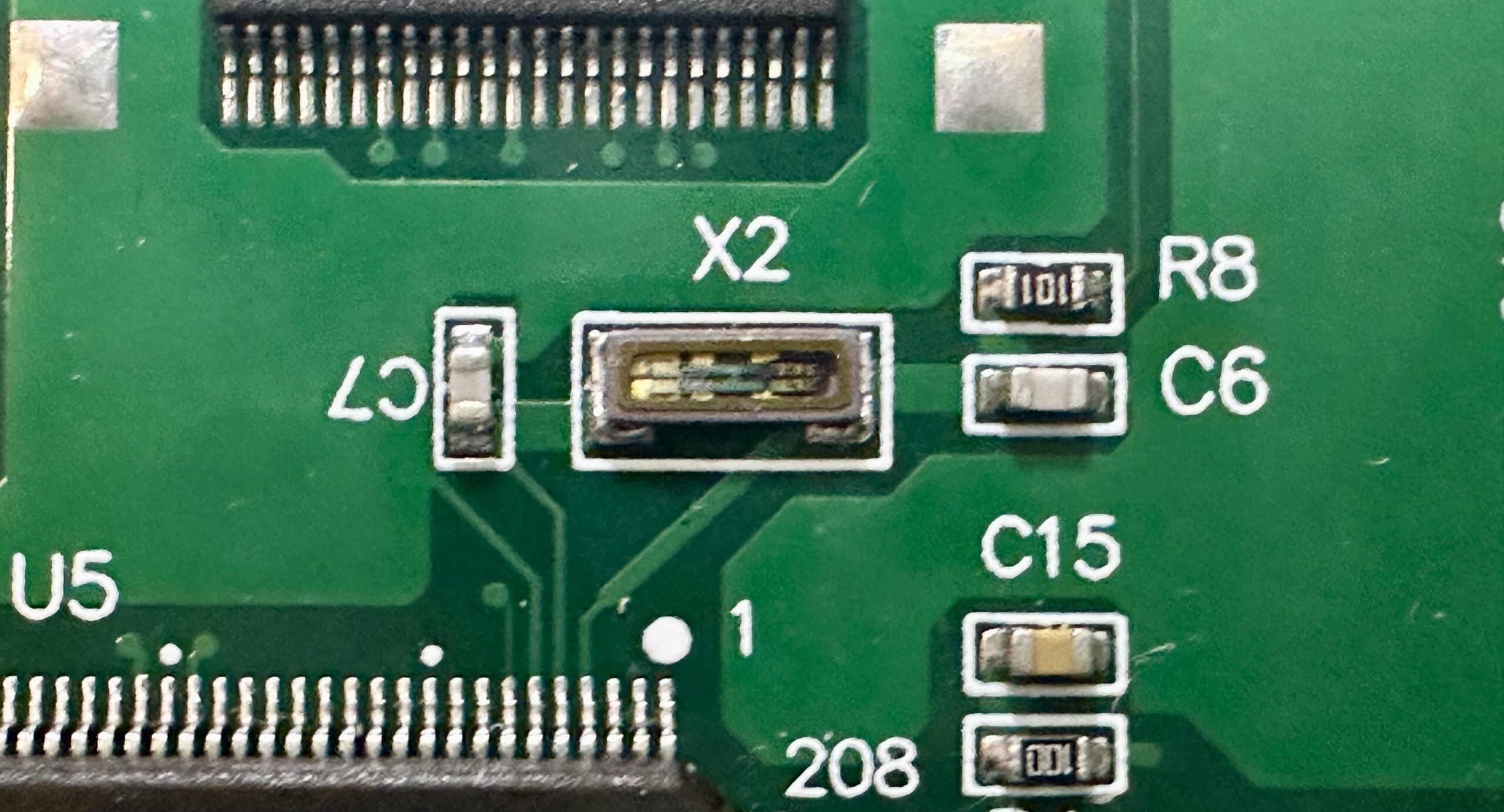
As per the CV1000 entry at the JAMMArcade.net PCB Encyclopedia, if D6 stays lit up, it indicates a problem with the clock generator located at position X2 on the board. Sure enough, the X2 part on this board is damaged – you can see right into it!
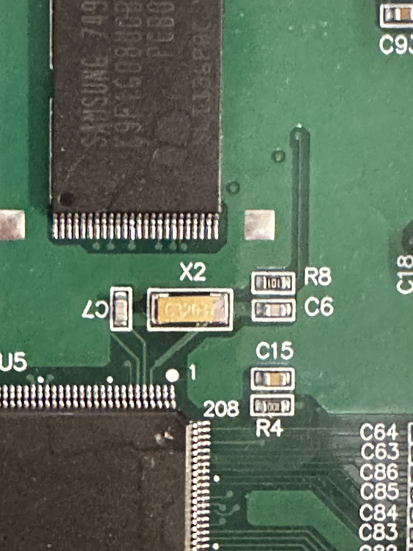
I sourced a replacement part from DigiKey. It is a 32.768 kHz crystal resonator measuring 4.9 mm X 1.8mm . Once the replacement part arrived, I used hot tweezers to remove the old crystal and then soldered the new one in.
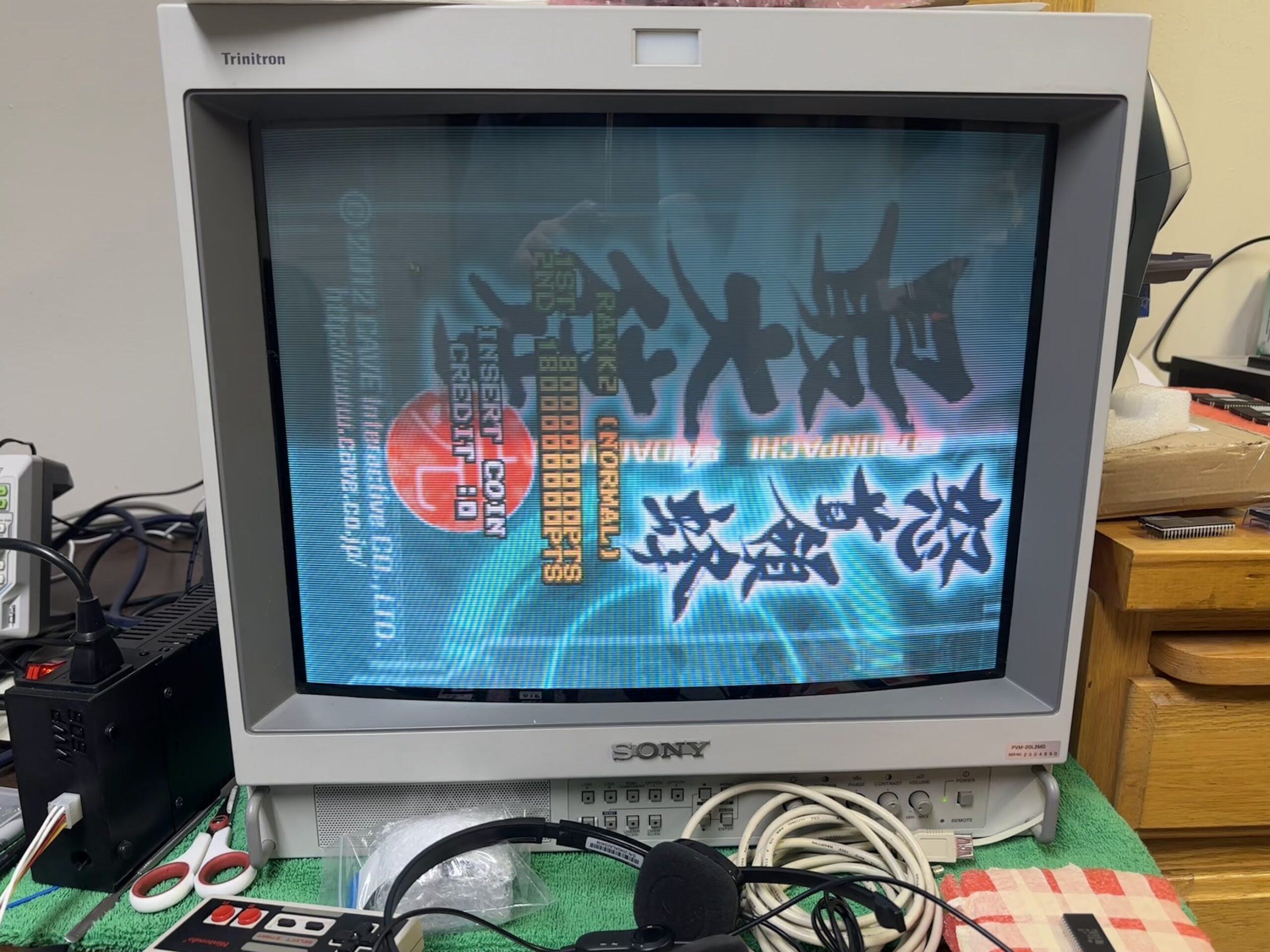
That’s all this board needed – with the new crystal in place, the game booted up and functioned perfectly. A successful repair!