Jul 172015
 

Im currently working on a Time Pilot PCB and tested out Shoestrings diagnostic ROM.
This board is the Atari version which wasnt supported at the time but has now been updated.
I also ran into a problem where nothing appeared on the screen. Working together we eventually found the issue.
The original game code makes a write of 01 to address $c308. Using the Fluke 9010 I found that this write actually initialises the screen output.
MAME doesnt have any support for this so when testing the ROM in MAME it works fine. The test ROM has been updated with this now too and should work fine.

This highlights the need to test things on REAL hardware.
Thanks to Shoestring for making the diagnostic ROM and for putting up with all my questions.

 Posted by at 5:04 pm

Taito F3 PALs confusion

 General, Technical Info  Comments Off on Taito F3 PALs confusion
Mar 142015
 

Back in January there was a discussion going on over on the Jamma+ forums regarding the D77-14 and D77-15 PAL dumps.
After a lot of help from various people and testing by myself here is the conclusion I have come to regarding this issue.

D77-14 is used when the main CPU ROM’s are 27c2001 (0x40000).
D77-15 is used when the main CPU ROM’s are 27c4001 (0x80000).

On a 27c2001 EPROM, pin 31 is the programming pin. It is active low so once the chip is programmed we want to keep this held high when in use. That’s exactly what the D77-14 PAL is doing. Pin 19 of this PAL is fixed HIGH and is connected to pin 31 of the 27c2001 EPROM.

On a 27c4001 EPROM, pin 31 not the programming pin but it is the upper most address bit and that’s why with a D77-15 pin 19 is able to toggle which allows for double sized EPROM’s to be used.

This is where the confusion comes in.
On many converted boards out there in the wild (and there is a lot of them) we have found there to be D77-14 stamped PAL chips with the same code as what we have found in D77-15 PAL chips and vice versa. Assuming the PAL chips themselves are the original ones from Taito (and I have no reason to see why they wouldn’t be) then my theory is, as they are all PALCE16V8 chips, which are reprogrammable, they have simply been reprogrammed by the bootlegger/converter to use whatever version they needed. This would keep it looking that little bit more authentic and also cuts down on the cost of buying a GAL16V8.

If you check in the MAME source too, every game that has program ROM’s of size 0x40000 uses the D77-14 PAL and every game that has program ROM’s of size 0x80000 uses a D77-15 PAL.

Hopefully that will clear up a bit of the confusion surrounding this.

Fluke 68000 POD ROM revisions

 General, Technical Info  Comments Off on Fluke 68000 POD ROM revisions
Mar 072015
 

Yesterday I received an email (and it was also posted on the UK-VAC forum) with some information on the 68000 POD firmware version.
Here is the info:

Fluke 68000 pod ROMS

U4.bin : 0x2361d749
U5.bin : 0xa6f59007
version 2.0

U4.bin : 0xa8859970
U5.bin : 0x486343c7
version 5.0 (this version is in https://www.jammarcade.net/fluke-pods/)

The version of a Fluke 68000 pod can be obtained by:

-Put the ribbon cable of the 68000 pod in the self test socket
-Press setup on the 9010a and check the following, changing if necessary:
SET-TRAP BAD POWER SUPPLY? YES
SET-TRAP ILLEGAL ADDRESS? YES
SET-TRAP ACTIVE INTERRUPT? NO
SET-TRAP ACTIVE FORCE LINE? NO
SET-TRAP CTL ERR? YES
SET-TRAP ADDR ERR? YES
SET-TRAP DATA ERR? YES
SET-ENABLE HALT? NO
SET-ENABLE BR/ACK? NO
SET-ENABLE INTR? NO

First disable the self-test performing WRITE @ F000 0028 = BF
and then do a READ of address F0000012, you get the value 0020 for version 2.0
and 0050 for version 5.0, this is explained in the 9000A-68000 Interface Pod manual in chapter 6-7.
If you get version 6.0 please let me know, this version has Quick Ramp, Quick Fill, Quick Verify
and the pattern verification option of Quick RAM.
PAL of version 2.0 pod is the same as of version 5.0 pod

If you want to re-enable the self-test, you can cycle pod power off and then on or do a WRITE @ F000 0028 = FF

Guddler had dumped his ROM’s some time ago when he was troubleshooting his pod and they didn’t match mine.
Based on the above information it would appear he has version 2 of the firmware and I have version 5.
I’ve amended the downloads section accordingly and also added Guddler’s dumps too for completeness.

If anyone has any other versions then it would be nice to get these too, especially the version 6 mentioned in the text above.

Oct 052014
 

Been doing a few bits with muddymusic’s Jumping PCB.
I wanted to see how the C-Chip substitute ROM was wired into the circuit so ive made a small schematic and reversed the address decoder PAL.
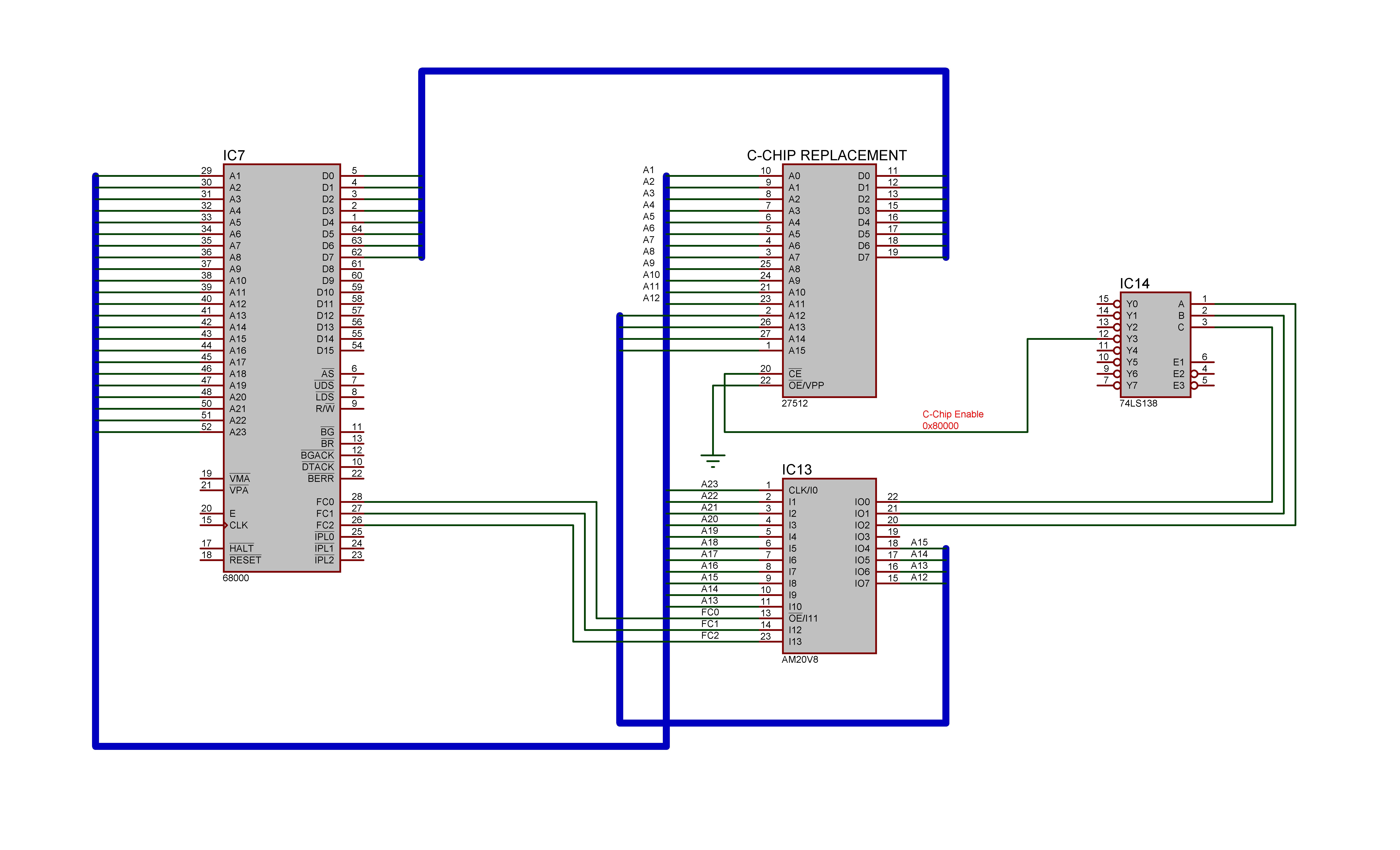
Jumping Schematics
click the pic for full size.

Here are the equations for the address decoder too. Ive renamed to the pins to something more suitable for human consumption.
/* Inputs */

Pin 1 = A23;
Pin 2 = A22;
Pin 3 = A21;
Pin 4 = A20;
Pin 5 = A19;
Pin 6 = A18;
Pin 7 = A17;
Pin 8 = A16;
Pin 9 = A15;
Pin 10 = A14;
Pin 11 = A13;
Pin 13 = FC0;
Pin 14 = FC1;
Pin 23 = FC2;

/* Outputs */

Pin 15 = CA12; /* A12 of C-Chip replacement ROM */
Pin 16 = CA13; /* A13 of C-Chip replacement ROM */
Pin 17 = CA14; /* A14 of C-Chip replacement ROM */
Pin 18 = CA15; /* A15 of C-Chip replacement ROM */
Pin 19 = LROM; /* Chip enable for other ROM’s */
Pin 20 = A; /* Pin 1 of 74LS138. Input A */
Pin 21 = B; /* Pin 2 of 74LS138. Input B */
Pin 22 = C; /* Pin 3 of 74LS138. Input C */

/* Equations */

!CA12 = !A23 & !A22 & !A21 & !A20 & !A19 & !A13 #
!A23 & !A22 & !A21 & A20 & !A19 & !A18 & !A17 & !A16 & A15 & A14 & !A13 #
!A23 & A22 & !A21 & !A20 & !A19 & !A18 & !A17 #
!A23 & A22 & !A21 & !A20 & !A19 & !A18 & A17 & A16 #
A23 & A22 & !A21 & !A20 & !A19 & !A18 & !A17 & !A16 & !A13 #
!A23 & !A22 & !A21 & !A20 & A19 & !A18 & !A17 & !A13 #
A23 & A22 & !A21 & A20 & !A19 & !A18 & !A17 & !A16 & !A15 & !A14 & !A13;

!CA13 = !A23 & !A22 & !A21 & !A20 & !A19 & !A14 #
!A23 & A22 & !A21 & !A20 & !A19 & !A18 & A17 #
A23 & A22 & !A21 & !A20 & !A19 & !A18 & !A17 & !A16 & !A14 #
!A23 & !A22 & !A21 & !A20 & A19 & !A18 & !A17 & !A14;

!CA14 = !A23 & !A22 & !A21 & !A20 & !A19 & !A15 #
A23 & A22 & !A21 & !A20 & !A19 & !A18 & !A17 & !A16 & !A15 #
!A23 & !A22 & !A21 & !A20 & A19 & !A18 & !A17 & !A15;

!CA15 = !A23 & !A22 & !A21 & !A20 & !A16;

!LROM = !A23 & !A22 & !A21 & !A20 & !A17;

!A = !A23 & !A22 & !A21 & !A20 & !A19 & !A18 #
!A23 & !A22 & !A21 & A20 & !A19 & !A18 & !A17 & !A16 & A15 & A14 #
!A23 & !A22 & A21 & !A20 & !A19 & !A18 & !A17 & !A16 & !A15 & !A14 & !A13 #
A23 & A22 & !A21 & !A20 & !A19 & !A18 & !A17 & !A16 #
A23 & A22 & !A21 & A20 & !A19 & !A18 & !A17 & !A16 & !A15 & !A14 & !A13;

!B = !A23 & !A22 & !A21 & !A20 & !A19 #
A23 & A22 & !A21 & !A20 & !A19 & !A18 & !A17 & !A16 #
!A23 & A22 & !A21 & !A20 & !A19 & A18 & !A17 & !A16 #
A23 & A22 & !A21 & A20 & !A19 & !A18 & !A17 & !A16 & !A15 & !A14 & !A13;

!C = !A23 & !A22 & !A21 & !A20 & !A19 #
!A23 & !A22 & !A21 & A20 & !A19 & !A18 & !A17 & !A16 & A15 & A14 #
!A23 & !A22 & !A21 & !A20 & A19 & !A18 & !A17;

The A, B and C outputs from the PAL feed into a 74LS138. In order to select the C-Chip substitute A and B must be HIGH and C must be LOW. From the equations (or just looking at the MAME source code) we can work out that the C-Chip ROM lies at address 0x80000.

So, not a great deal of info but its pretty interesting all the same.

Jul 202014
 

At the moment I have an X Multiply PCB that shows a “RAM NG 10” error on startup.
Although I have yet to find the problem with this board I thought it best to find out exactly what RAMs these errors are referring to.
To make any sense of this you will need the memory map for the game found in M72.C file of the MAME source code.

Here is a short list of what I have found so far:
0x9c000-0x9ffff = RAM NG 1 (Work RAM)
0xc0000-0xc03ff = RAM NG 10 (Sprite RAM)
0xc8000-0xc8bff = RAM NG 9 (Palette RAM 1)
0xcc000-0xccbff = RAM NG 8 (Palette RAM 2)
0xd0000-0xd3fff = RAM NG (Video RAM 1)
0xd8000-0xdbfff = RAM NG (Video RAM 2)

 Posted by at 8:30 pm