
Received an ESP Ra.De. board for repair for my friend Vic.
This was the video I was sent originally
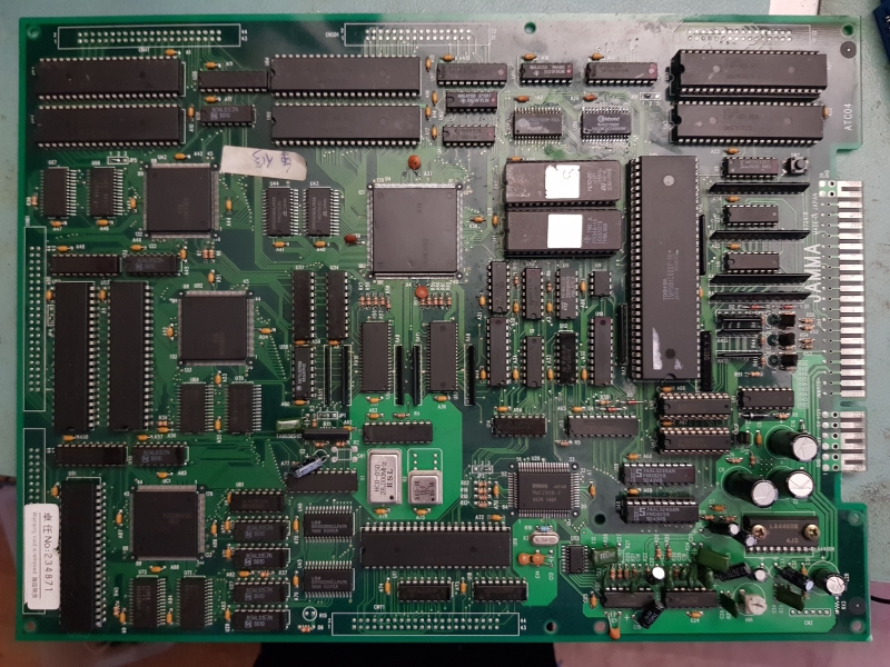
This PCB had apparently had work done before but all we knew was the big 240 pin custom chip had been reflowed. This always makes me nervous because if it was destroyed somehow then all further attempts of repair would be for nothing unless I had a donor.
Visual check carried out of the board in general revealed nothing bad so hooked it up to the test. As expected we have no sync and the game does not appear to be running either. I confirmed this as the watchdog was kicking in.
Using the scope I probed the sync pin at the JAMMA connector and found a low sync signal of 13khz.
I started tracing the signal back but it went to the big custom chip that I already knew had been worked on, I also confirmed the main clocks and signal to the custom chip.
With no other ideas at this point I decided to tackle the game booting issue. The 68000 CPU was already in a socket so using the Fluke 9010 with a 68000 POD (Thanks Caius for the extended loan of his POD) I could start troubleshooting.
First off a BUS check revealed data bit 2 was tied low. In actual fact data bits 2 and 3 were shorted together.
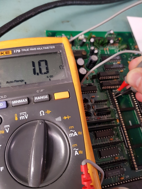
I started tracing all the point where these data lines go and one by one started isolating them from the circuit. Once again my search led back to this big custom chip.
Reflowing these two pins on the custom cleared the fault.
At this point I took a closer look at this custom and found if I got the light in at the right angle I could see a lot of dried flux underneath.
Over time flux residue will dry out if not properly cleaned and it can go conductive.
I cleaned this and the bus test now passes. The ROM check between 0x0 – 0x7FFFF should be 1BBA which also passed.
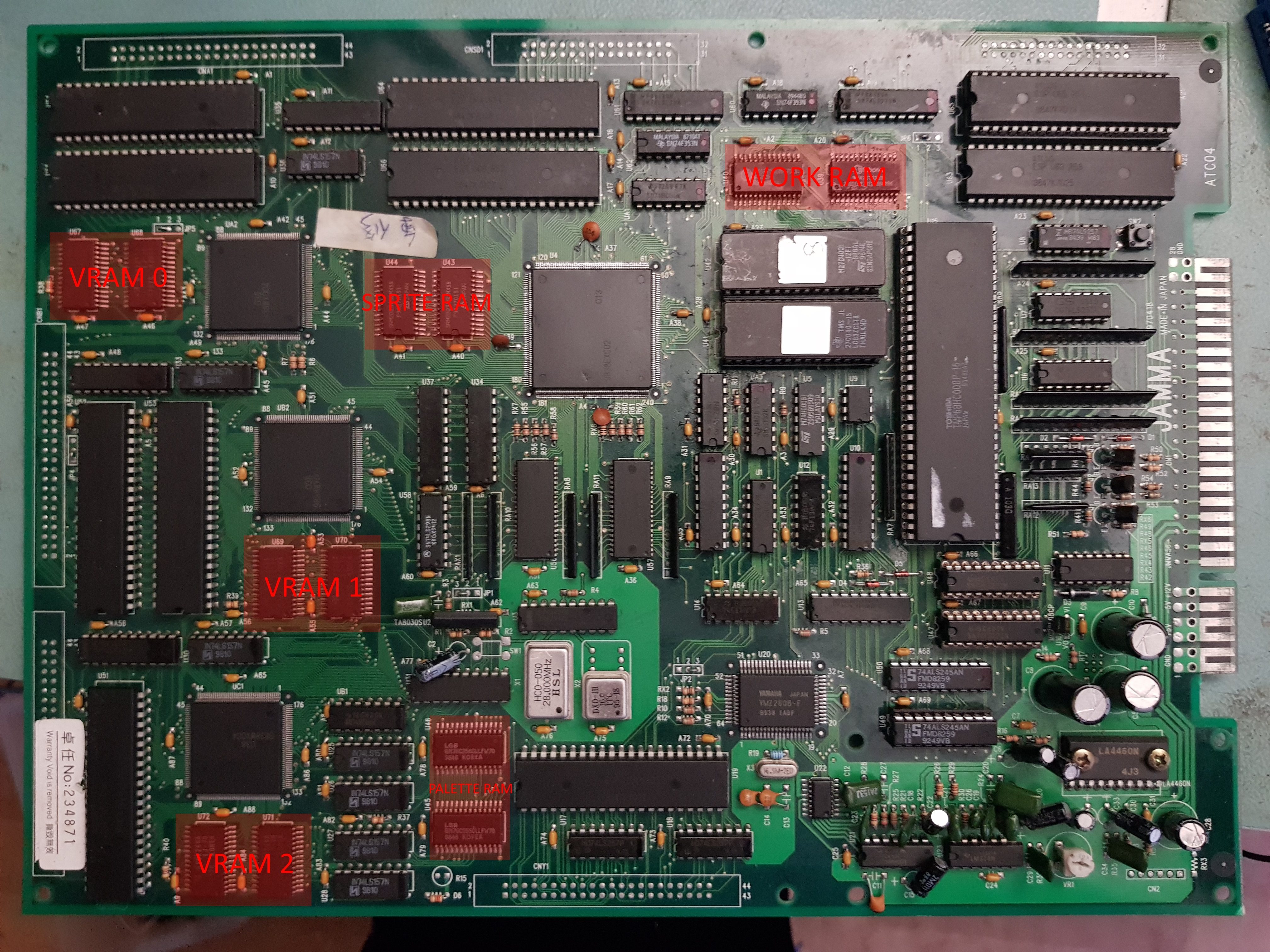
The main RAM lies at location U39 & U40, 0x100000, 0x10FFFF. The Fluke reported a decode error on bit 1 which basically means there is a problem with the address lines.
Doing some manual reads and writes I could see that bit 1 of RAM U39 did not work. I replaced this and retested which then went OK.
I started my way through the rest of the RAM location as per the MAME driver.
The sprite RAM lies at U43 & U44, 0x400000, 0x40FFFF. Once again the fluke reported bits 5 & 6 tied together and once again I was led back to the same custom chip.
From here I just opted to reflow the whole chip. This cleared the issue with the sprite RAM. All other VRAM passed tests.
Retesting the PCB now resulted in a nice looking game for the most part but there was a strange strobing around test and lines that were white. Going into the test mode made this very obvious.
I couldn’t get a good video of this as it all looked fine on a camera.
To began with I thought this was all to do with my test monitor and the sync being a tiny bit high for it but I tested it on all my monitors and cabs and they all gave strange results.
I eventually went back to that custom chip and inspected all the pins again.
I couldn’t visually see anything but checking continuity on all pins against the adjacent pins revealed a short somewhere around pin 190. A further reflow of these pins resulted in a completed repair
One strange thing about this board is that on boot up it stays in a reset state for around 2 seconds which is the point where the sync reads 13khz. After that the sync steps up to 15.23khz and all OK.
Here is a layout of all the RAM locations on the PCB
Sorry, the comment form is closed at this time.