Heavy Unit repair log #2

 PCB Repair Logs, Repair Logs  Comments Off on Heavy Unit repair log #2
Feb 062016
 

Got this pcb to be repaired from a friend.

The pcb was working perfect excepts that the screen was flickering at 1/2 of the vsync.

As usual I visually inspected the board to find loose legs on smd chips but the only one present was good.

I noticed that the pcb had 4x rams 4164 near the video custom chip which are known to be not very reliable.

I started to probe the rams until I found one which had all the signals very weaks.

After soldering a new one, the problem was fixed!

Heavy Unit

Heavy Unit repair log #1

 PCB Repair Logs, Repair Logs  Comments Off on Heavy Unit repair log #1
Dec 142015
 

I got a dead Heavy Unit PCB with a white screen on boot:

hvyunit1

Looking at the MAME driver for that game I could see where the program roms were located (5C for the main program rom and 5P for the sub program rom).
I started probing around the CPUs and program roms. The CPUs (2 x Z80) seemed active and the program roms had pulsing signals on most of their pins. A few were inactive and connected to nearby GALs (labeled MD-500 and MD-501). All the I/O pins were stuck low on these two GALs while they had pulsing inputs.

There are 3 GALs in total on that board, MD-500 is connected to the main program rom, MD-501 is connected to the sub program rom and MD-502 is connected to the sound rom.
Surprisingly all these 3 GALs had inactive I/O pins. I got a working Heavy Unit PCB from a friend, compared the signals on the GALs and saw that almost every I/O pins were pulsing on the 3 GALs.

These GALs were not available online so I started desoldering them on both PCBs.
I put sockets on the dead PCB, socketed the GALs from the working board and the game booted ! …but with partially missing graphics (I had colored squares instead of sprites):

hvyunit2

Looking at the PCB I supposed the main program rom at 5C was not original as it had no label. Dumping it revealed it was from a US version. Looking at the MAME driver, I could see that every of the 4 versions dumped in MAME had a different ROM layout and my version was not dumped (the numbers on the labels were not in MAME). Particularly, there was a 512kb ROM at 2F on every versions in MAME that wasn’t soldered on my PCB, although I found its content spread on 4x128kb ROMs at other locations. The main program ROM was probably looking at the wrong location so I soldered a socket at 2F to put the 512kb ROM (from one of the MAME dumped versions and labeled B73_08) and the sprites were back. 🙂

hvyunit3

Here is my PCB with the added 512kb EPROM from MAME at 2F (equivalent to B73_17 + B73_18 + B73_19 + B73_20 on the left):

hvyunit0

ps: I’m still looking for the original program ROM for my PCB (labeled B73_24 and located at 5C) to be dumped so I could remove the 512kb at 2F and use the original 128kb ROMs already present on the board. I suppose it is a japanese version.

ps2: I wanted to dump the GALs from the working board but they were protected. To dump protected GALs I needed to use a method by Charles MacDonald. First, I used this adapter in order to read my GALs as 27C020 EPROMs: https://techno-junk.org/files/adapter-v2.png
Then, I used PD.EXE and WinCUPL to recreate the GALs from my raw dumps: https://dreamjam.co.uk/emuviews/readpal.php
These GALs are now available on https://www.jammarcade.net

Jun 242015
 

Got this pcb from ebay marked with “cracking sound problems”

The game sounded like an old LP with a lot of scratches and missed some sounds.

On this board, the YM2610 handle FM synthesis and PCM samples.

Given the fact that it is very difficult that the sound chip will fail, I started to probe the smd stereo DAC YM3016.

I could hear the same cracked sound coming out and I was sure that changing it would fix the issues.

I found a donor board and soldered a new DAC.


Foto 16-05-15 10 49 00

Retested the pcb and same problems.

At this time I was quite sure that the sound chip itself was broken.

Suddendly I remembered the most obvious thing to test first: the sound rom C43-01!

It was a maskrom….marked Taito….they had the most unreliable supplier ever.

In the past, I found many Taito maskroms which caused gfx faults because of internal faults.

After cheking the maskrom on my eprom programmer one pin was not making contact and it was clear that is was an internal break.

Burning a 4mbit eprom with maskrom pinout (like a 27c4100) restored the sound.


Foto 16-05-15 10 49 31

Oct 052014
 

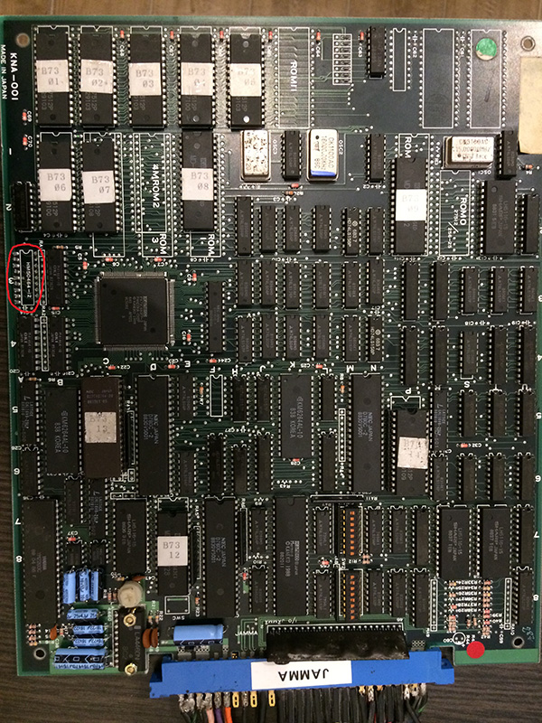
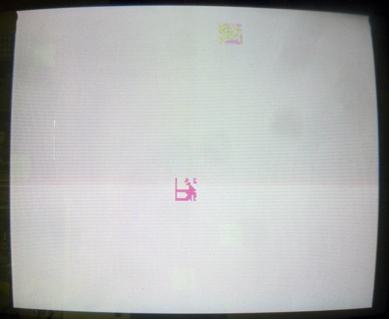
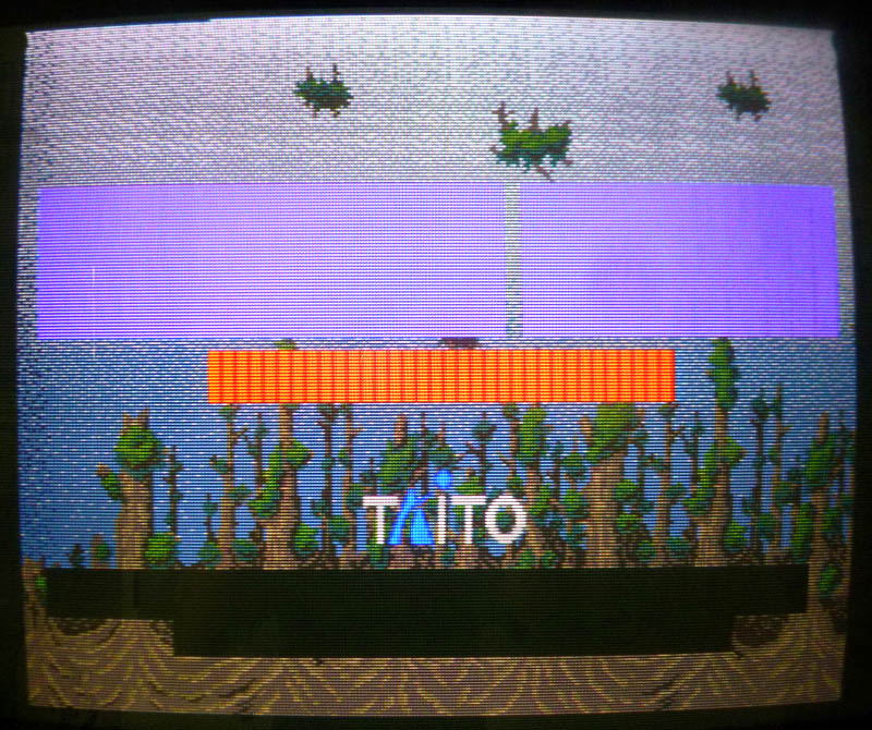
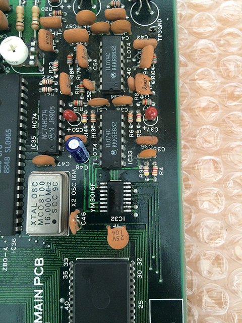
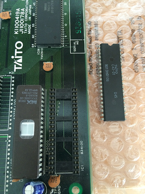
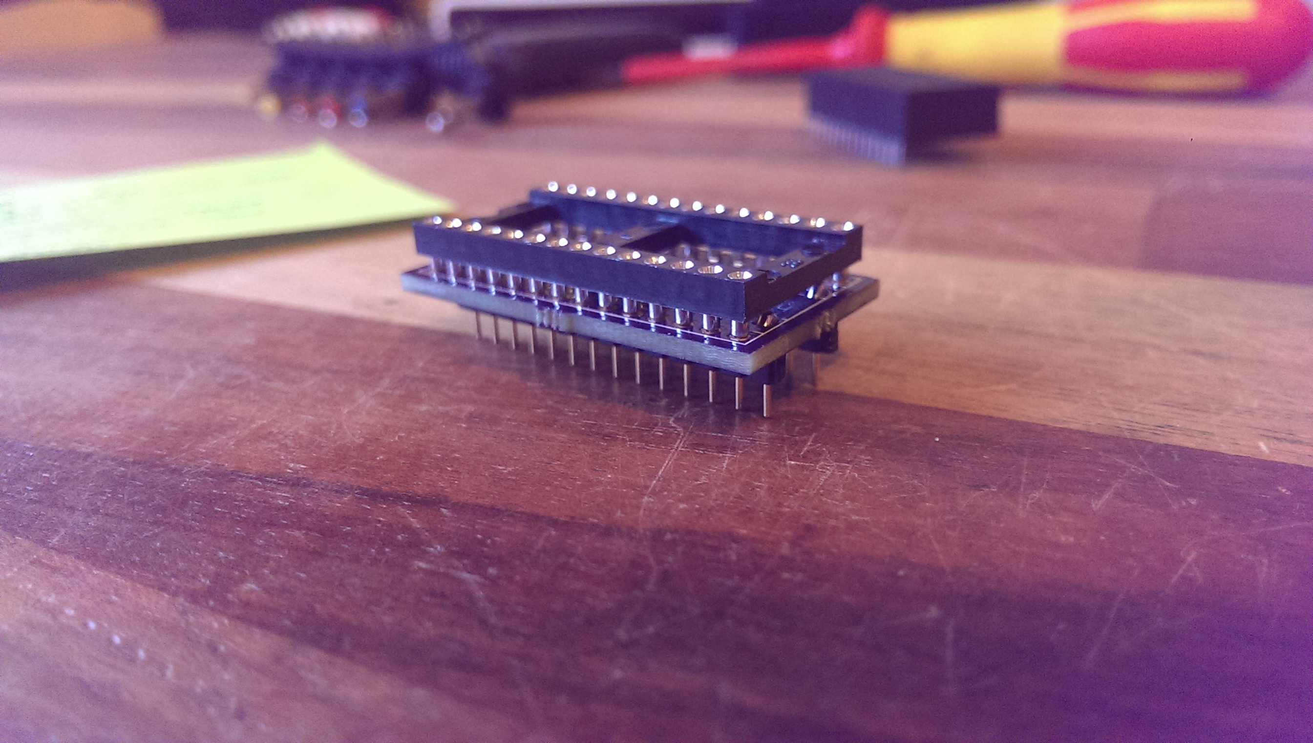
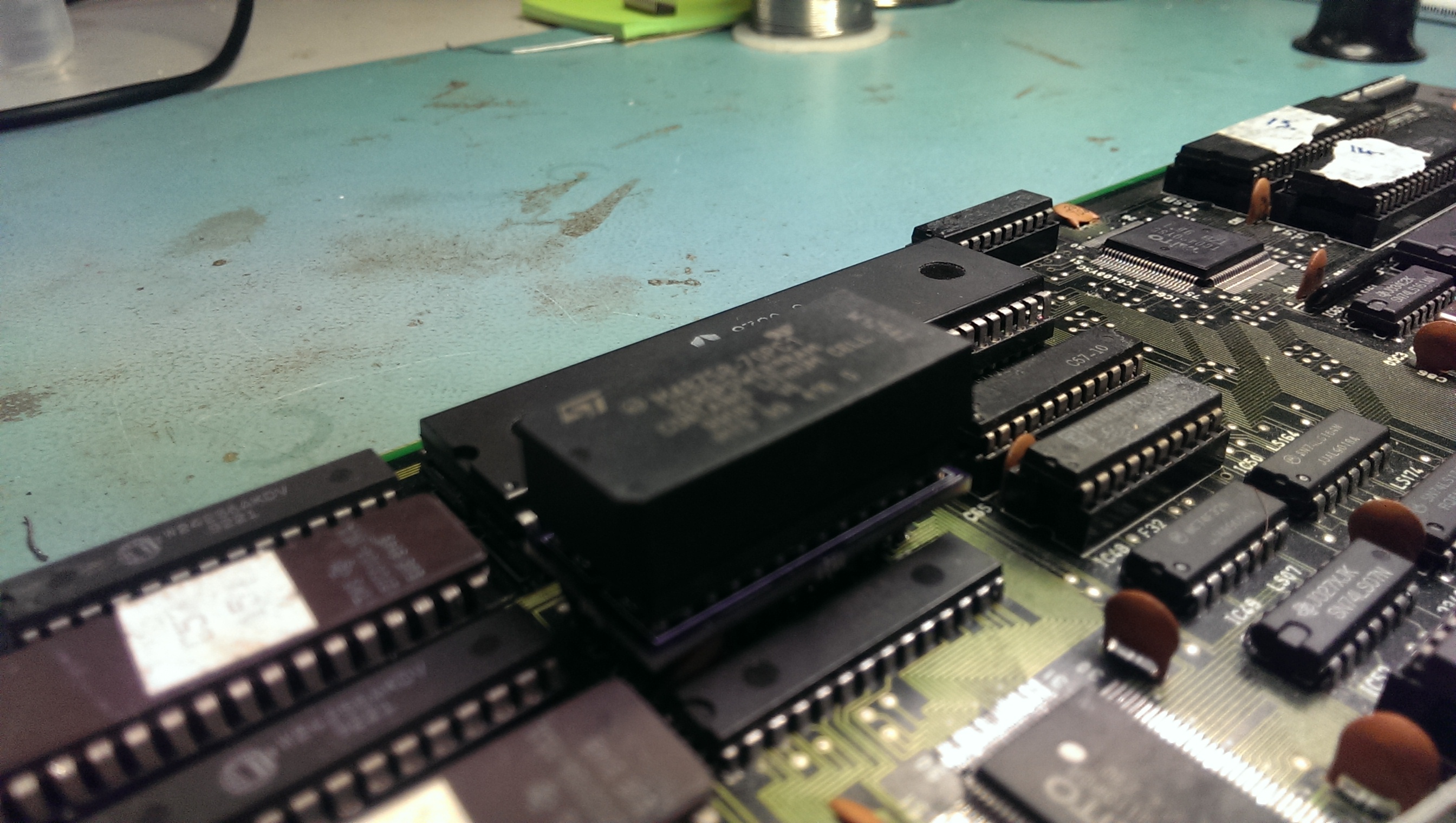
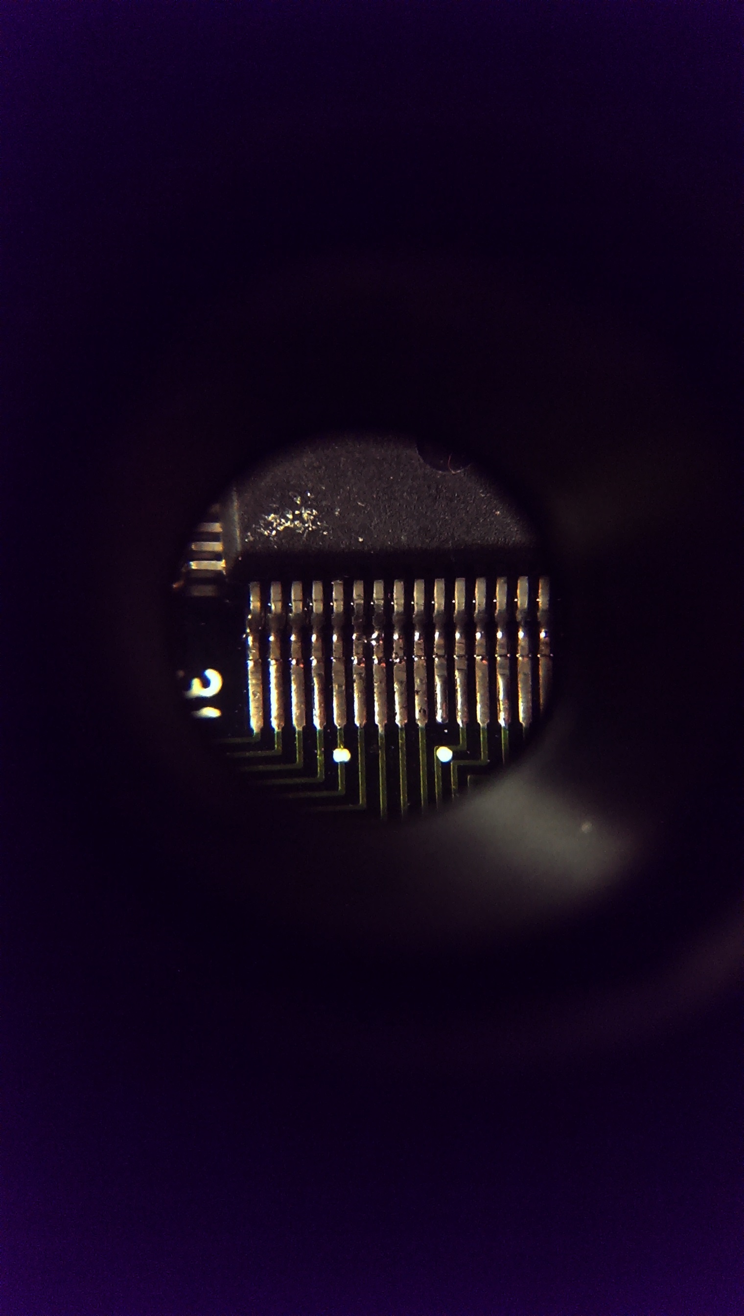
Been doing a few bits with muddymusic’s Jumping PCB.
I wanted to see how the C-Chip substitute ROM was wired into the circuit so ive made a small schematic and reversed the address decoder PAL.

Jumping Schematics
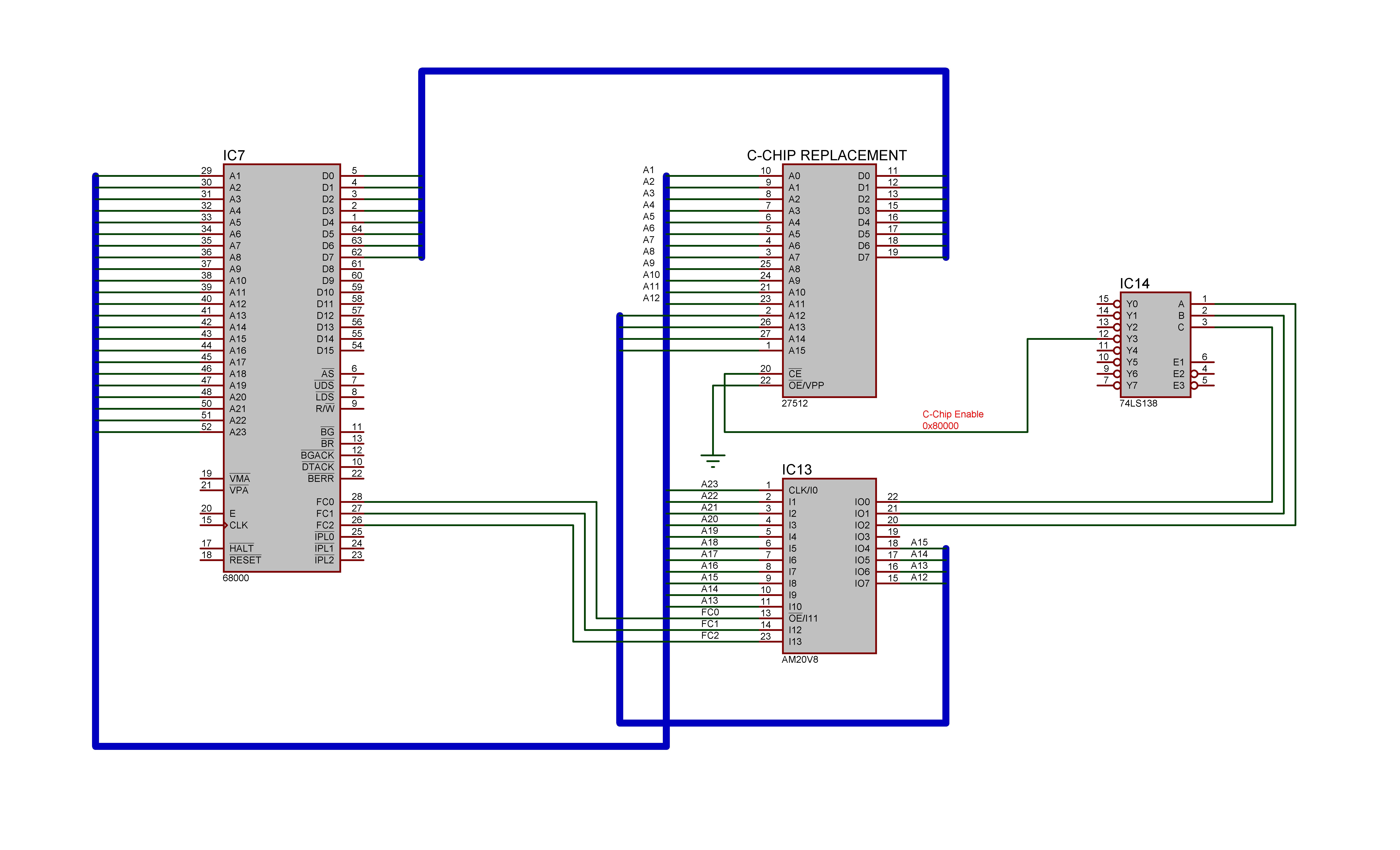
click the pic for full size.

Here are the equations for the address decoder too. Ive renamed to the pins to something more suitable for human consumption.
/* Inputs */

Pin 1 = A23;
Pin 2 = A22;
Pin 3 = A21;
Pin 4 = A20;
Pin 5 = A19;
Pin 6 = A18;
Pin 7 = A17;
Pin 8 = A16;
Pin 9 = A15;
Pin 10 = A14;
Pin 11 = A13;
Pin 13 = FC0;
Pin 14 = FC1;
Pin 23 = FC2;

/* Outputs */

Pin 15 = CA12; /* A12 of C-Chip replacement ROM */
Pin 16 = CA13; /* A13 of C-Chip replacement ROM */
Pin 17 = CA14; /* A14 of C-Chip replacement ROM */
Pin 18 = CA15; /* A15 of C-Chip replacement ROM */
Pin 19 = LROM; /* Chip enable for other ROM’s */
Pin 20 = A; /* Pin 1 of 74LS138. Input A */
Pin 21 = B; /* Pin 2 of 74LS138. Input B */
Pin 22 = C; /* Pin 3 of 74LS138. Input C */

/* Equations */

!CA12 = !A23 & !A22 & !A21 & !A20 & !A19 & !A13 #
!A23 & !A22 & !A21 & A20 & !A19 & !A18 & !A17 & !A16 & A15 & A14 & !A13 #
!A23 & A22 & !A21 & !A20 & !A19 & !A18 & !A17 #
!A23 & A22 & !A21 & !A20 & !A19 & !A18 & A17 & A16 #
A23 & A22 & !A21 & !A20 & !A19 & !A18 & !A17 & !A16 & !A13 #
!A23 & !A22 & !A21 & !A20 & A19 & !A18 & !A17 & !A13 #
A23 & A22 & !A21 & A20 & !A19 & !A18 & !A17 & !A16 & !A15 & !A14 & !A13;

!CA13 = !A23 & !A22 & !A21 & !A20 & !A19 & !A14 #
!A23 & A22 & !A21 & !A20 & !A19 & !A18 & A17 #
A23 & A22 & !A21 & !A20 & !A19 & !A18 & !A17 & !A16 & !A14 #
!A23 & !A22 & !A21 & !A20 & A19 & !A18 & !A17 & !A14;

!CA14 = !A23 & !A22 & !A21 & !A20 & !A19 & !A15 #
A23 & A22 & !A21 & !A20 & !A19 & !A18 & !A17 & !A16 & !A15 #
!A23 & !A22 & !A21 & !A20 & A19 & !A18 & !A17 & !A15;

!CA15 = !A23 & !A22 & !A21 & !A20 & !A16;

!LROM = !A23 & !A22 & !A21 & !A20 & !A17;

!A = !A23 & !A22 & !A21 & !A20 & !A19 & !A18 #
!A23 & !A22 & !A21 & A20 & !A19 & !A18 & !A17 & !A16 & A15 & A14 #
!A23 & !A22 & A21 & !A20 & !A19 & !A18 & !A17 & !A16 & !A15 & !A14 & !A13 #
A23 & A22 & !A21 & !A20 & !A19 & !A18 & !A17 & !A16 #
A23 & A22 & !A21 & A20 & !A19 & !A18 & !A17 & !A16 & !A15 & !A14 & !A13;

!B = !A23 & !A22 & !A21 & !A20 & !A19 #
A23 & A22 & !A21 & !A20 & !A19 & !A18 & !A17 & !A16 #
!A23 & A22 & !A21 & !A20 & !A19 & A18 & !A17 & !A16 #
A23 & A22 & !A21 & A20 & !A19 & !A18 & !A17 & !A16 & !A15 & !A14 & !A13;

!C = !A23 & !A22 & !A21 & !A20 & !A19 #
!A23 & !A22 & !A21 & A20 & !A19 & !A18 & !A17 & !A16 & A15 & A14 #
!A23 & !A22 & !A21 & !A20 & A19 & !A18 & !A17;

The A, B and C outputs from the PAL feed into a 74LS138. In order to select the C-Chip substitute A and B must be HIGH and C must be LOW. From the equations (or just looking at the MAME source code) we can work out that the C-Chip ROM lies at address 0x80000.

So, not a great deal of info but its pretty interesting all the same.

Oct 022014
 

To start with this game wouldn’t boot at all.
The board has had one of its big surface mount custom chips replaced in the past and apart from one lifted track that has been patched out, the swap was very neat.
First job was to desolder the sub CPU and fit the Fluke to see what was going on.
I found a broken link between the ROMs and D4 of the CPU. I patched this and did a ROM check.

The ROM address space lies between 0x0-0x3ffff.
The Fluke 9010 signature for this is 8A4F

This was correct but the game still refused to boot.
Checked the RAM. This lies between addresses 0x20C000-0x20FFFF
Both of these failed and both were replaced.
Ram checks now pass but the game still does not boot.

Next I tested the shared RAM.
This lies between 0x210000-0x21FFFF
This passed up until address 0x21FFFE where I couldn’t write to the address at all.
I haven’t figured out why but I’m starting to think this is normal as the code writes to this address space separately but never reads from it. Maybe some kind of watchdog reset or something?

As the game still did not boot I opted to desolder the main CPU and fit the Fluke there.
Found another broken track between the main CPU and one of the ROM’s (I forgot which one as this repair has taken ages).
I patched this out and the game now boots but there is a faint output on screen. Further probing with the scope revealed a dead TC0070 RGB custom chip.
I replaced this and now got a booting game but with wrong colours.
IMAG0883

IMAG0885

This had me stumped for a while as there are a lot of custom chips on this board and any one of them could be a suspect as they all feed into and out of each other.
I opted for a different approach to normal and made up a small converter PCB that let me use 0.6″ chips in place of 0.3″ chips. This allowed me to use an NVRAM chip in place of the palette RAM.
IMAG0948

IMAG0933
So with this in place I let the game boot to the title screen and powered off. With the contents stored in the NVRAM I was able to dump it and repeat the operation for the second palette RAM and interleave the dumps together. No I had this I could compare it to what MAME has at the same point. This allowed me to see if the data being written was actually correct or not.

Here is what I got on my first attempt and what I should have got.
SGwrong
SGright

As you can hopefully see, bits 4 and 6 are wrong here so I took a closer look at the custom chip TC0110PCR that feeds the RAM chips.
IMAG0934

There was the smallest bridge of solder across D6 and D7. Removing this gave me the colours back.
IMAG0944

IMAG0945

Everything else appears to be working so I am glad this is now sorted.